Electrode substrate, photoelectric conversion element, conductive glass substrate and production method therefo, and pigment sensitizing solar cell

a technology of photoelectric conversion and conductive glass, which is applied in the direction of electrolytic capacitors, final product manufacture, sustainable manufacturing/processing, etc., can solve the problems of marked deterioration of transmission light ratio, and deterioration of photoelectric conversion efficiency of solar cells, so as to prevent corrosion and leakage current effectively, the effect of excellent conductivity

Active Publication Date: 2006-07-27
THE FUJIKURA CABLE WORKS LTD
View PDF8 Cites 98 Cited by
  • Summary
  • Abstract
  • Description
  • Claims
  • Application Information

AI Technical Summary

Benefits of technology

[0019] According to this electrode substrate, it is ensured that the metal circuit layer is shielded from an electrolyte solution and the like, and corrosion thereof and leak current can be effectively prevented. Thus, the electrode substrate exhibits excellent conductivity.
[0020] The insulating layer is preferably made of a material that contains a glass component, and is particularly preferably formed by printing a paste that contains glass frit. By this, it is possible to easily form an insulating layer that reliably insulates...

Problems solved by technology

Consequently, commercially available transparent conductive glass has a high resistance, and when it is used for solar cells, in particular, when it is used for large surface area cells, there is a marked deterioration in the photoelectric conversion efficiency.
However, the photoabsorption by a transparent conductive layer increases if the film is formed having a thickness large enough to allow a satisfactory resistance to be obtained, and the ratio of transmitted light deteriorates markedly.
By this, the photoelectric conversion efficiency of the solar cell also deteriorates.
However, because the surfaces of the transparent conductive layer 611 and the metal circuit layer 612 present profiles having minute bumps and irregularities such as voids, cracks, and particle boundaries, it is difficult for a dense shielding layer 613 to be formed uniformly, and there are cases in which uncovered portions in which the metal circuit layer 612 is exposed are generated by incomplete formation of the shielding layer 613.
For example, when the metal circuit layer 612 is formed using a conductive paste that includes conductive particles such as fine metal particles and a bonding agent such as glass frit as the main components, from the viewpoint of the conductivity of the metal circuit layer 612, it is preferable that the compounding ratio of the bonding agent be low, however, minute and sharp bumps and irregularities and shadow portions such as voids and pinholes tend to be generated on the interior and surface of the metal circuit layer 612, so that forming a shading layer is difficult.
Because of this, there may be a reduction in the current collecting efficiency, and the cell characteristics may be impaired markedly.
Because these tend to cause corrosion of the circuit and reverse electron transfer to the electrolyte solution and the like, the cell characteristics m...

Method used


Image

  • Electrode substrate, photoelectric conversion element, conductive glass substrate and production method therefo, and pigment sensitizing solar cell
  • Electrode substrate, photoelectric conversion element, conductive glass substrate and production method therefo, and pigment sensitizing solar cell
  • Electrode substrate, photoelectric conversion element, conductive glass substrate and production method therefo, and pigment sensitizing solar cell

Examples


example a1

(Manufacturing of an Electrode Substrate)

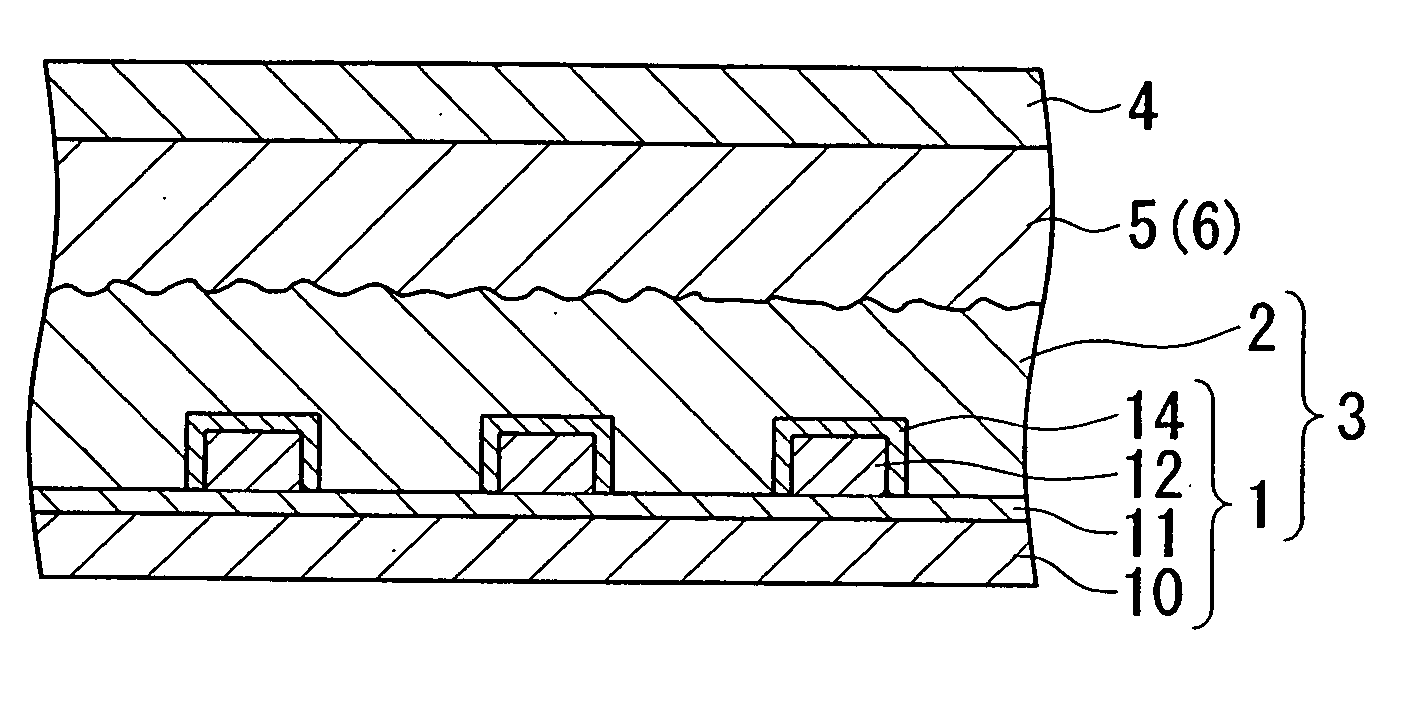
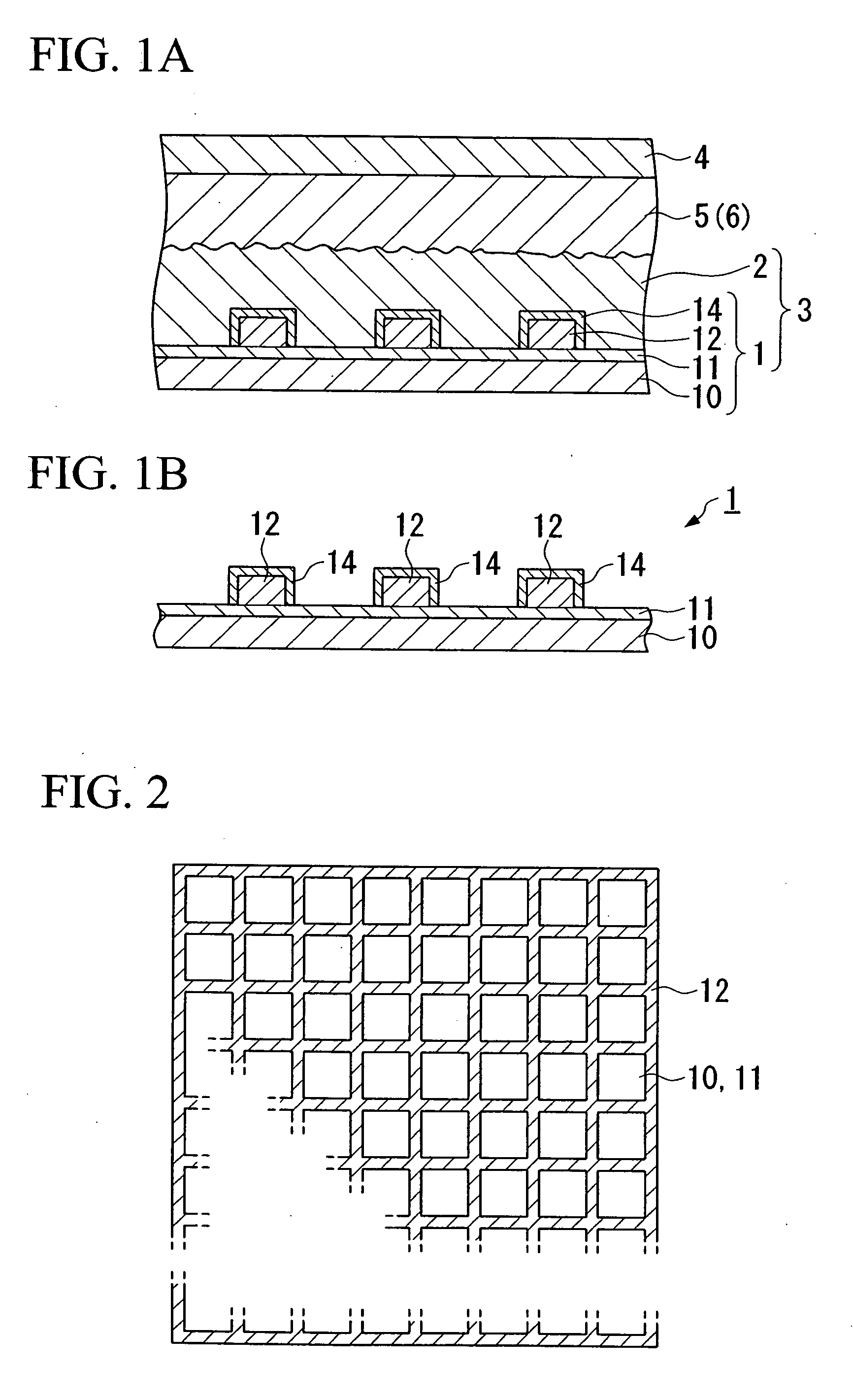
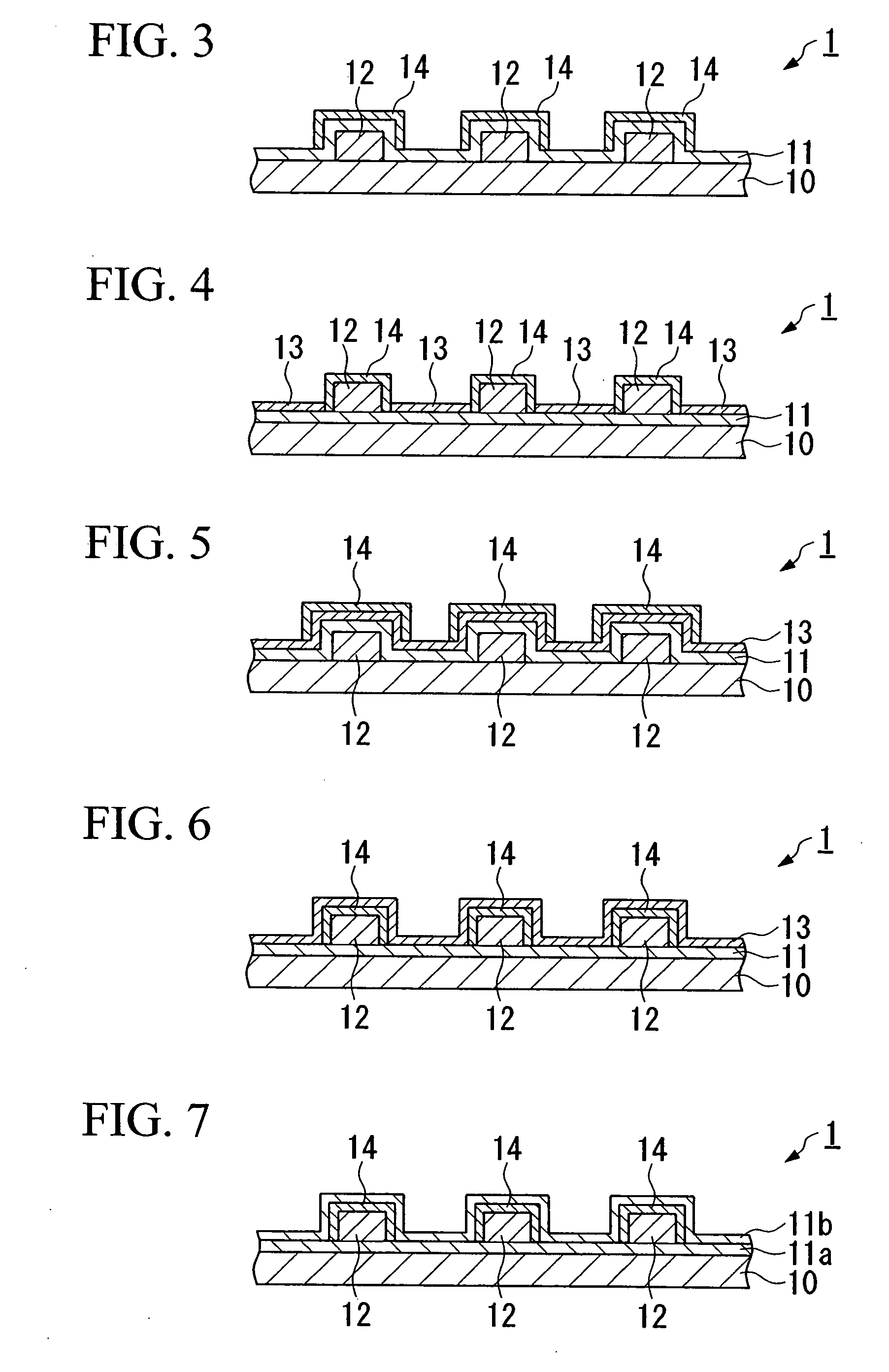
[0100] A 100 mm×100 mm glass substrate provided with an FTO film was used as a transparent conductive layer 11 (11a) and the base material 10. A silver printing paste (having a volume resistivity after baking of 3×10⁻⁶Ω) was screen printed on the surface thereof in a lattice pattern. After 10 minutes of leveling, the paste was dried in a hot air circulating furnace at 135° C. for 20 minutes, and was then baked at 550° C. for 15 minutes so as to form the metal circuit layer 12 having a silver circuit. The circuit width of the metal circuit layer 12 was 150 μm, while the film thickness was 5 μm.

[0101] Glass paste was printed overlapping the metal circuit layer 12 by screen printing while alignment was conducted using a CCD camera. After 10 minutes of leveling, the paste was dried in a hot air circulating furnace at 135° C. for 20 minutes, and was then baked at 550° C. for 15 minutes so as to form the insulating layer 14. The width of the ins...

example a2

(Manufacturing of an Electrode Substrate)

[0107] A 100 mm×100 mm heat-resistant glass substrate was used as the base material 10. Using the same procedure as in Example A1, a metal circuit layer 12 having a circuit width of 50 μm and a film thickness of 5 μm was formed on the surface of the substrate using a silver printing paste. Next, an FTO film that was the transparent conductive layer 11 was formed on the metal circuit layer 12 by an SPD method. Furthermore, using the same procedure as in Example A1, the insulating layer 14 was formed by printing glass paste so that the insulating layer 14 corresponds to the pattern of the metal circuit layer 12. As a result, the electrode substrate 3 having the structure shown in FIG. 3 was manufactured.

(Manufacturing of a Photoelectric Conversion Element)

[0108] Using this electrode substrate 1, a photoelectric conversion element was manufactured for use as a test cell using the same procedure as in Example A1. When the photoelectric conve...

example a3

(Manufacturing of Electrode Substrate)

[0109] A 100 mm×100 mm glass substrate provided with an FTO film was used as the transparent conductive layer 11 and the base material 10. A metal circuit layer 12 with a gold circuit having a circuit width of 50 μm and a film thickness of 5 μm was formed on the surface of the transparent conductive layer 11 by an additive plating method. Next, using the same procedure as in Example A1, the insulating layer 14 was formed on top of the metal circuit layer 12 by printing glass paste so that the insulating layer 14 corresponds to the pattern of the metal circuit layer 12. As a result, the electrode substrate 1 having the structure shown in FIG. 1B was manufactured.

(Manufacturing of Photoelectric Conversion Element)

[0110] Using this electrode substrate 1, a photoelectric conversion element was manufactured for use as a test cell using the same procedure as in Example A1. When the photoelectric conversion characteristics of this test cell were e...


PUM


Abstract

In an electrode substrate 1, the surface of a metal circuit layer 12 is covered and insulated by an insulating layer 14. In a photoelectric conversion element that uses this electrode substrate 1, the metal circuit layer is reliably shielded from an electrolyte solution or the like so that corrosion and leak current thereof is effectively prevented, and the photoelectric conversion efficiency can be improved. The insulating layer 14 is preferably made of a material that contains a glass component, and is particularly preferably formed by printing a paste that contains glass frit. The metal circuit layer 12 is preferably formed using a printing method.

Description

TECHNICAL FIELD [0001] The present invention relates to an electrode substrate and a conductive glass substrate that are used in a photoelectric conversion element, and to a photoelectric conversion element, and a dye-sensitized solar cell. BACKGROUND ART [0002] Dye-sensitized solar cells are attracting attention as photoelectric conversion elements that are low in cost and enable a high conversion efficiency to be obtained (see, for example, Japanese Unexamined Patent Application, First Publication No. H01-220380; and Michael Graetzel, Nature, United Kingdom, 1991, vol. 737, p. 353). Generally, in this type of photoelectric conversion element, a semiconductor electrode is constructed by forming a porous film with oxide semiconductor nanoparticles of titanium dioxide or the like on a transparent conductive substrate, and then causing a sensitizing dye to be provided in this porous film. This semiconductor electrode is used with a counter electrode made of conductive glass that has b...

Claims


Application Information

Patent Timeline
IPC IPC(8): H01L31/00H01G9/20H01M14/00
CPCH01G9/2031Y02E10/542H01L51/445H01G9/2068Y02P70/50H10K30/83H01L31/04H01M14/00H01L31/18
Inventor MATSUI, HIROSHIOKADA, KENICHIKAWASHIMA, TAKUYATANABE, NOBUOEZURE, TETSUYA
Owner THE FUJIKURA CABLE WORKS LTD
Why Eureka
Try Eureka