Amorphous carbon contact film for contact hole etch process

Inactive Publication Date: 2006-08-03
TAIWAN SEMICON MFG CO LTD
View PDF1 Cites 43 Cited by
  • Summary
  • Abstract
  • Description
  • Claims
  • Application Information

AI Technical Summary

Benefits of technology

[0007] To achieve the foregoing and other objects, and in accordance with the purposes of the present invention, as embodied and broadly described herein, the present invention

Problems solved by technology

One problem in the prior art process is unintentional yet difficult to avoid removal of underlying critical material layers during dry etching process step in a uniform manner, such as silicide regions and (shallow trench isolation (STI) oxide regions, for example at the STI edge.
As a result, the formation of shallow source/drain junctions is increasingly problematical due to the difficulty in controlling overetch phenomenon in nitride etch stop layers.
For example overetching under

Method used


Image

  • Amorphous carbon contact film for contact hole etch process
  • Amorphous carbon contact film for contact hole etch process
  • Amorphous carbon contact film for contact hole etch process

Examples


Example

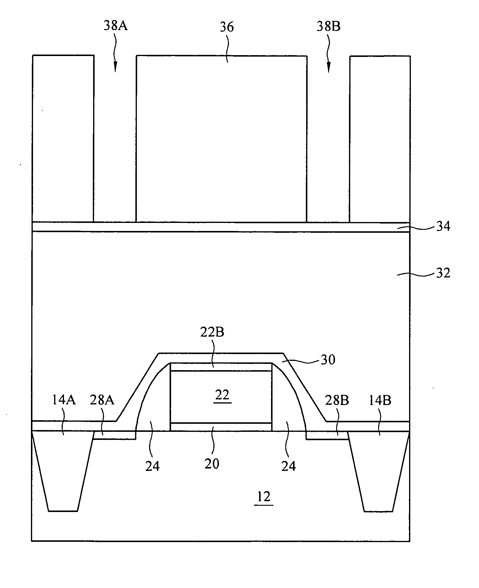
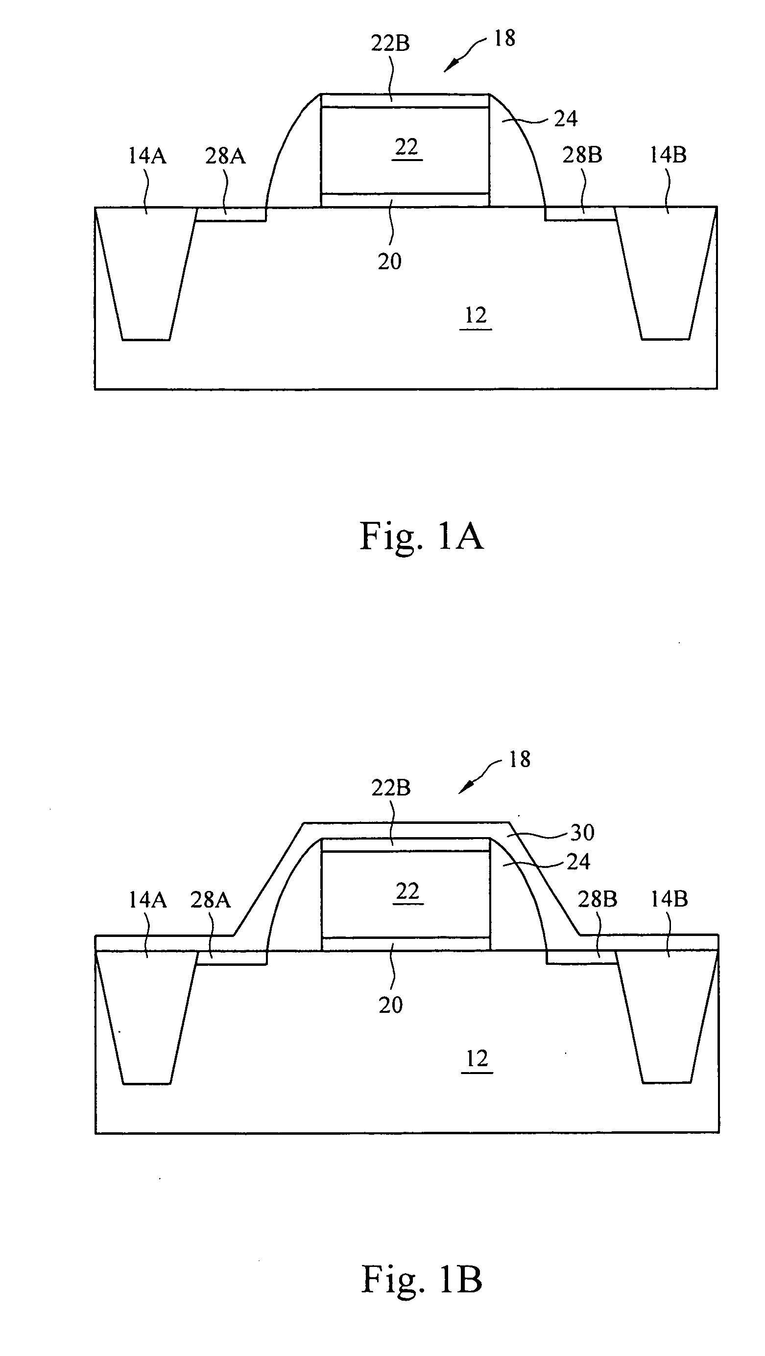
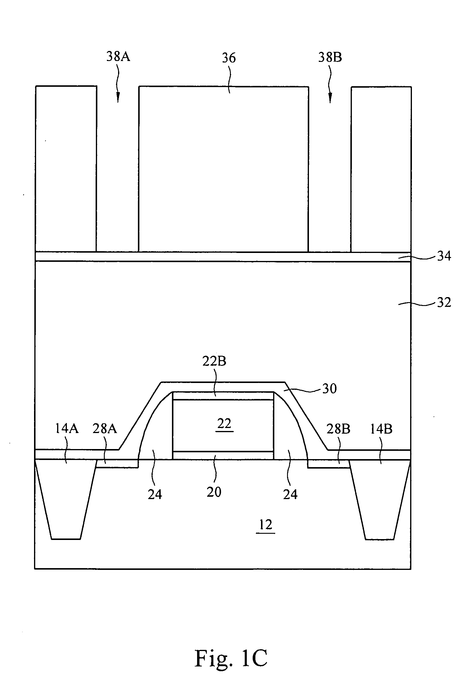
[0012] Although the method of the present invention is explained with reference to an exemplary MOSFET devices, it will be appreciated that the present invention may be applied to the formation of any CMOS device whereby a contact etch stop layer formed of fluorine doped amorphous carbon is provided allowing improved device performance as well as the advantageous implementation of the associated contact hole formation process to reduce loss of critical underlying material including silicided CMOS device contact regions and shallow trench isolation (STI) regions.

[0013] Now, referring to FIG. 1A, is shown a semiconductor substrate 12, which may include silicon, strained semiconductor, compound semiconductor, multi-layered semiconductors, or combinations thereof. More specifically, the substrate 12 may include, but is not limited to, silicon on insulator (SOI), stacked SOI (SSOI), stacked SiGe on insulator (S—SiGeOI), SiGeOI, and GeOI, or combinations thereof. In a preferred embodimen...


PUM


Abstract

A semiconductor device including a contact etch stop layer and contact hole formation method for reduced underlying material loss and improved device performance, the method including providing a semiconductor substrate including an active region including a CMOS device, STI structures, and metal silicide regions; forming a fluorine doped amorphous carbon layer over the active region; forming a PMD layer on the fluorine doped amorphous carbon layer; dry etching contact holes in the PMD layer to expose the fluorine doped amorphous carbon layer; and, removing the fluorine doped amorphous carbon layer according to a dry stripping process.

Description

FIELD OF THE INVENTION [0001] This invention generally relates to formation of MOSFET devices by integrated circuit manufacturing processes and more particularly to a contact film structure and method of forming the same including a contact hole etch process to reduce material loss of underlying layers including silicide contact regions and / or STI oxide regions. BACKGROUND OF THE INVENTION [0002] In the integrated circuit industry today, millions of semiconductor transistors are built on a single chip. As CMOS transistors, also referred to as MOSFETs, are scaled down in size, one of the most important challenges facing a device designer are short channel effects (SCE) in reduced gate length devices. It is well-known that short channel effects of MOSFET devices include VT roll-off, drain induced barrier lowering (DIBL), subthreshold swing degradation, gate-to-drain overlap capacitance and gate-induced-drain-leakage (GIDL) current. Short channel effects (SCE) are a function of several...

Claims


Application Information

Patent Timeline
IPC IPC(8): H01L29/78H01L21/8238
CPCH01L21/0212H01L21/02266H01L21/31116H01L21/31122H01L21/31138H01L21/3127H01L21/31608H01L21/31625H01L21/76802H01L21/76829H01L21/76834H01L21/76897H01L21/823871H01L29/78H01L29/7843Y02P80/30
Inventor CHIANG, WEN-CHUANCHEN, CHENG-KUCHIANG, MU-CHICHI, MIN-HWA
Owner TAIWAN SEMICON MFG CO LTD
Why Eureka
Try Eureka