Supercritical fluid-assisted deposition of materials on semiconductor substrates

a technology of supercritical fluid and semiconductor substrate, which is applied in the direction of liquid/solution decomposition chemical coating, chemical vapor deposition coating, coating, etc., can solve the problems of limited cvd process for film deposition, high particle level, and low thermal stability of many chemical species

Inactive Publication Date: 2006-08-10
XU CHONGYING +2
View PDF26 Cites 22 Cited by
  • Summary
  • Abstract
  • Description
  • Claims
  • Application Information

AI Technical Summary

Benefits of technology

[0146] SCFD has certain advantages over both CVD and PVD in that there is no need for expensive, potentially toxic, highly volatile precursors or high processing temperatures as are necessary in CVD and PVD. Further, SCFD readily achieves high concentrations of precursor, far higher than those attainable in CVD, due to the solvating power of the SCF component(s). These factors, along with the lower deposition temperatures enabled by SCFD, enable such method to achieve faster processing times and subsequent reduction in process costs.

Problems solved by technology

However, many chemical species are neither thermally stable enough, nor volatile enough, for sustained vaporization, delivery and deposition.
As a consequence, CVD processes for film deposition are largely limited by the availability of volatile and stable precursors as source reagents.
PVD, utilizing a charged gas and a sputter target to effect deposition of material on a substrate, is well-developed and widely used in the art, but is limited by the significant particle levels that are generated in the process, as well as by constraints on controllability and conformality of the deposition process when tight geometries and small features are involved, and by process control issues relating to diffusion of the sputtered material.
Due to the ballistic nature of sputtered materials, it is extremely difficult to achieve conformal coverage on complex topography of next generation patterned substrates.
Physical vapor deposition is currently a preferred technique for depositing high purity metal films, but conventional PVD methods tend to produce thin bottom-corner coverage in deep vias or trenches, thereby producing a potential weak point for barrier performance.
Since aspect ratios are a critical factor in evolving device microstructures, it is likely that in the very near future the PVD technique will not be able to provide sufficient step coverage to deposit the diffusion barrier at the required thickness at all points within the high aspect ratio via.
Although many of such processes are extremely well-developed for advanced microelectronic device manufacture, the application of these processes for high aspect ratio via filling is burdened by difficulties.
For deposition of conducting materials such as copper, CVD processes therefore can only compete with electroplating techniques (aqueous based processes) when the cost of ownership (COO) for the process is small.
However, low equilibrium vapor pressure of available precursors and mass-transfer-limited kinetics in the CVD and ECD processes, respectively, leads to poor control over the deposition process.
Additionally, copper diffuses readily into oxides and dielectrics, causing line-to-line leakage.
Moreover, the copper can readily react with silicon at temperatures below 200° C., causing detrimental effects that can ultimately lead to device failure.
Further, the dielectric constant of the low k material is critical and aqueous contamination can negatively increase dielectric constants, which is largely unacceptable.
With decreasing feature size and increasing aspect ratio, the use of PVD to obtain the required seed layers becomes a major technical challenge.
Alkyl siloxanes and cyclosiloxanes such as TMCTS (tetramethylcyclotetrasiloxane) and OMCTS (octamethylcyclotetrasiloxane) are promising precursors for deposition of such films, but are susceptible to the presence of trace amounts of impurities that can lead to undesirable cationic or anionic polymerization.
For example, TMCTS polymerizes in delivery lines at temperatures above ˜120° C. Polymerization of such reagents can produce occlusion of reagent delivery lines and associated equipment, with catastrophic consequences in the semiconductor processing facility.
Unfortunately, there are few known materials with dielectric constants this low, and none of such known materials is compatible with semiconductor manufacturing requirements.
The utilization of porous insulator polymeric materials, however, introduces a new and unique set of integration issues.
The deficiencies of CVD-grown low k polymeric materials include premature degradation and / or polymerization of the precursors in delivery lines caused by the high temperatures typically employed, as discussed hereinabove, with the potential for catastrophic consequences within the processing tool.
However, thin films of controlled stoichiometry are somewhat difficult to fabricate.
For example, it is very difficult to deposit a PZT film directly on an Si substrate because Pb is highly reactive with Si and easily diffuses into the Si substrate.
This leads to an increase in complexity of the overall process as well as an increase in cost.
PVD methods, however, have the associated disadvantages of physical damage to the dielectric during sputtering of the metal films and metal diffusion through the dielectric material in the device structure.

Method used


Image

  • Supercritical fluid-assisted deposition of materials on semiconductor substrates

Examples


Embodiment Construction

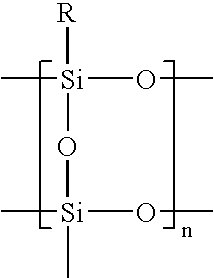
[0030] Supercritical fluids are formed under conditions at which the density of the liquid phase equals the density of the gaseous phase of the substance. For example, carbon dioxide (CO2), which is a gas at standard temperature and pressure, undergoes a transition from liquid to SCF above a critical point, corresponding to Tc≧31.1° C. and pc≧73.8 atm. Once formed, the density of the SCF can be varied from liquid-like to gaseous-like, yielding different solvation abilities, by varying the pressure and temperature. Supercritical fluids have a solubility and diffusibility approaching that of the liquid and gaseous phase, respectively. Additionally, the surface tension of SCFs is negligible.

[0031] Because of its readily manufactured character, ability to be recycled, lack of toxicity and negligible environmental effects, supercritical CO2 is a preferred SCF in the broad practice of the present invention, although the invention may be practiced with any suitable SCF species, with the c...


PUM

PropertyMeasurementUnit
thicknessaaaaaaaaaa
temperaturesaaaaaaaaaa

Abstract

Supercritical fluid-assisted deposition of materials on substrates, such as semiconductor substrates for integrated circuit device manufacture. The deposition is effected using a supercritical fluid-based composition containing the precursor(s) of the material to be deposited on the substrate surface. Such approach permits use of precursors that otherwise would be wholly unsuitable for deposition applications, as lacking requisite volatility and transport characteristics for vapor phase deposition processes.

Description

CROSS REFERENCE TO RELATED APPLICATIONS [0001] This is a continuation of the U.S. Patent Application No. 10 / 632,009 for “Supercritical Fluid-Assisted Deposition of Materials on Semiconductor Substrates” filed on Jul. 31, 2003 in the name of Chongying Xu et al., which is incorporated herein in its entirety. CROSS-REFERENCE TO RELATED APPLICATION [0002] This is a continuation-in-part of U.S. patent application no. 10 / 303,479 filed Nov. 25, 2002, which in turn claims the priority of U.S. provisional patent application no. 60 / 345,738 filed Dec. 31, 2001. [0003] 1. Field of the Invention [0004] The present invention relates generally to using supercritical fluids to effect the deposition of materials on substrates, e.g., semiconductor substrates, in the manufacture of semiconductor devices and device precursor structures. [0005] 2. Description of the Related Art [0006] In the field of semiconductor manufacturing, deposition of materials on semiconductor substrates is carried out by a var...

Claims


Application Information

Patent Timeline
Patent Type & Authority Applications(United States)
IPC IPC(8): H01L21/4763C23C16/16C23C16/18C23C16/34C23C16/44C23C16/448C23C18/00C23C18/12H01LH01L21/288H01L21/312H01L21/316H01L21/768
CPCC23C18/00H01L2924/0002C23C18/1204C23C18/1208C23C18/1212C23C18/1216C23C18/122C23C18/1275H01L21/02126H01L21/02203H01L21/02216H01L21/02282H01L21/288H01L21/3121H01L21/31695H01L21/76801H01L21/76841H01L21/76877C23C18/08H01L2924/00
Inventor XU, CHONGYINGBAUM, THOMAS H.KORZENSKI, MICHAEL B.
Owner XU CHONGYING
Why Eureka
Try Eureka