Oxynitride phosphor and semiconductor light-emitting device

a technology of oxynitride phosphor and light-emitting device, which is applied in the direction of discharge tube luminescent screen, discharge tube/lamp details, luminescent composition, etc., can solve the problems of insufficient stability that have not yet been found, and achieve excellent heat resistance, excellent emission efficiency, and less material deterioration and brightness deterioration

Active Publication Date: 2006-08-24
SHARP KK +1
View PDF2 Cites 79 Cited by
  • Summary
  • Abstract
  • Description
  • Claims
  • Application Information

AI Technical Summary

Benefits of technology

[0033] The oxynitride phosphor according to the invention exhibits brightness higher than that of an existing sialon phosphor, in particular, it can efficiently emit light of a wavelength of 510 nm or less. Furthermore, since the oxynitride phosphor according to the invention is mainly made of an oxynitride phosphor excellent in the heat resistance, when it is exposed to light excitation, in comparison with other general phosphor materials, material deterioration and brightness deterioration are less.
[0034] Furthermore, the oxynitride phosphor according to the invention, when it is excited by light having a wavelength of 390 nm or more and 420 nm or less where the photo-electric conversion efficiency is highest in a semiconductor light-emitting element such as a LED or laser that has an active layer made of for instance InGaN, has excellent emission efficiency. Accordingly, a semiconductor light-emitting device that uses the oxynitride phosphor according to the invention has high emission efficiency as a whole.

Problems solved by technology

However, a phosphor that is excellent in the emission efficiency of light from blue to bluish purple mainly made of wavelengths of 510 nm or less and has sufficient stability has not yet been found.

Method used


Image

  • Oxynitride phosphor and semiconductor light-emitting device
  • Oxynitride phosphor and semiconductor light-emitting device
  • Oxynitride phosphor and semiconductor light-emitting device

Examples


examples 1 through 10

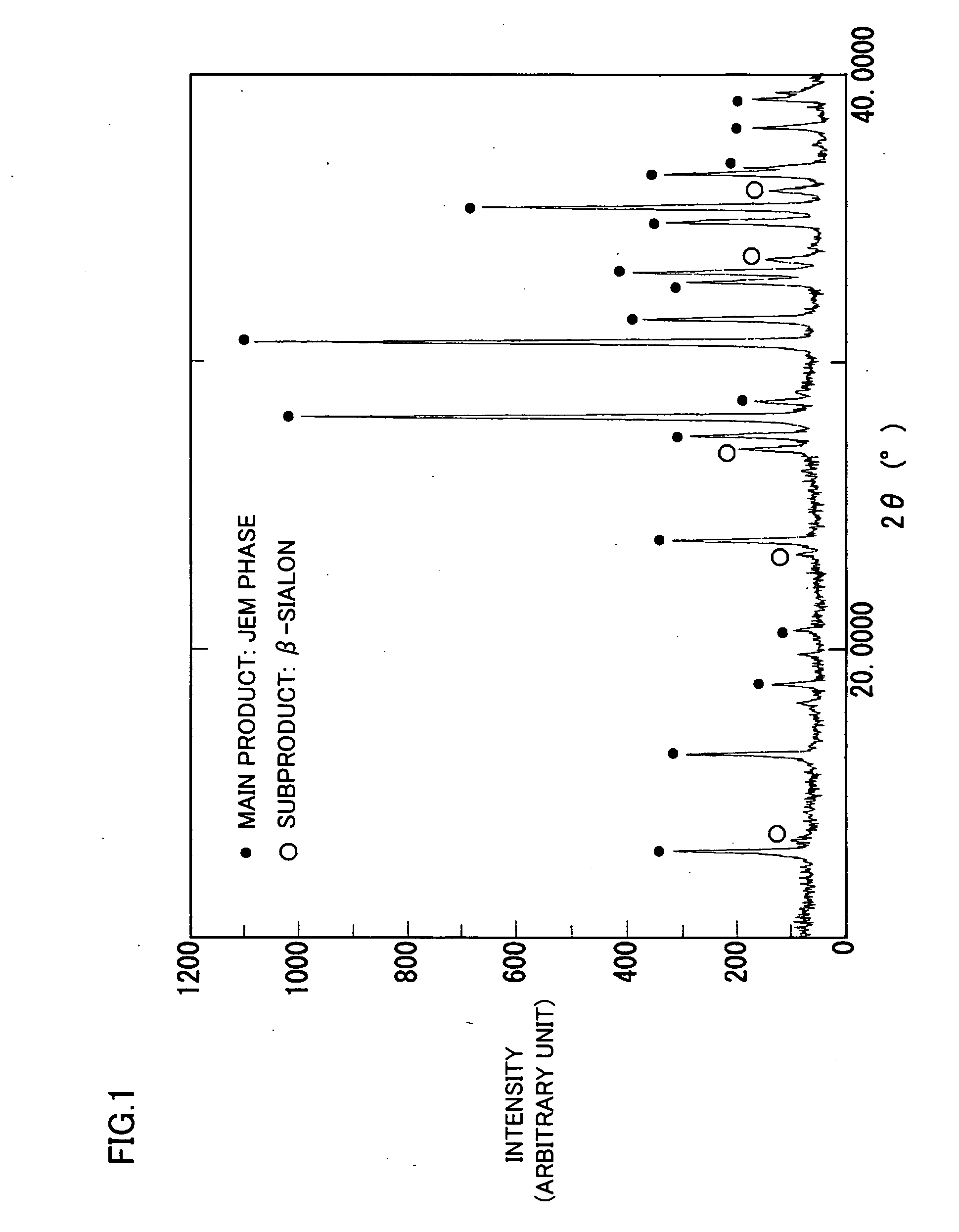
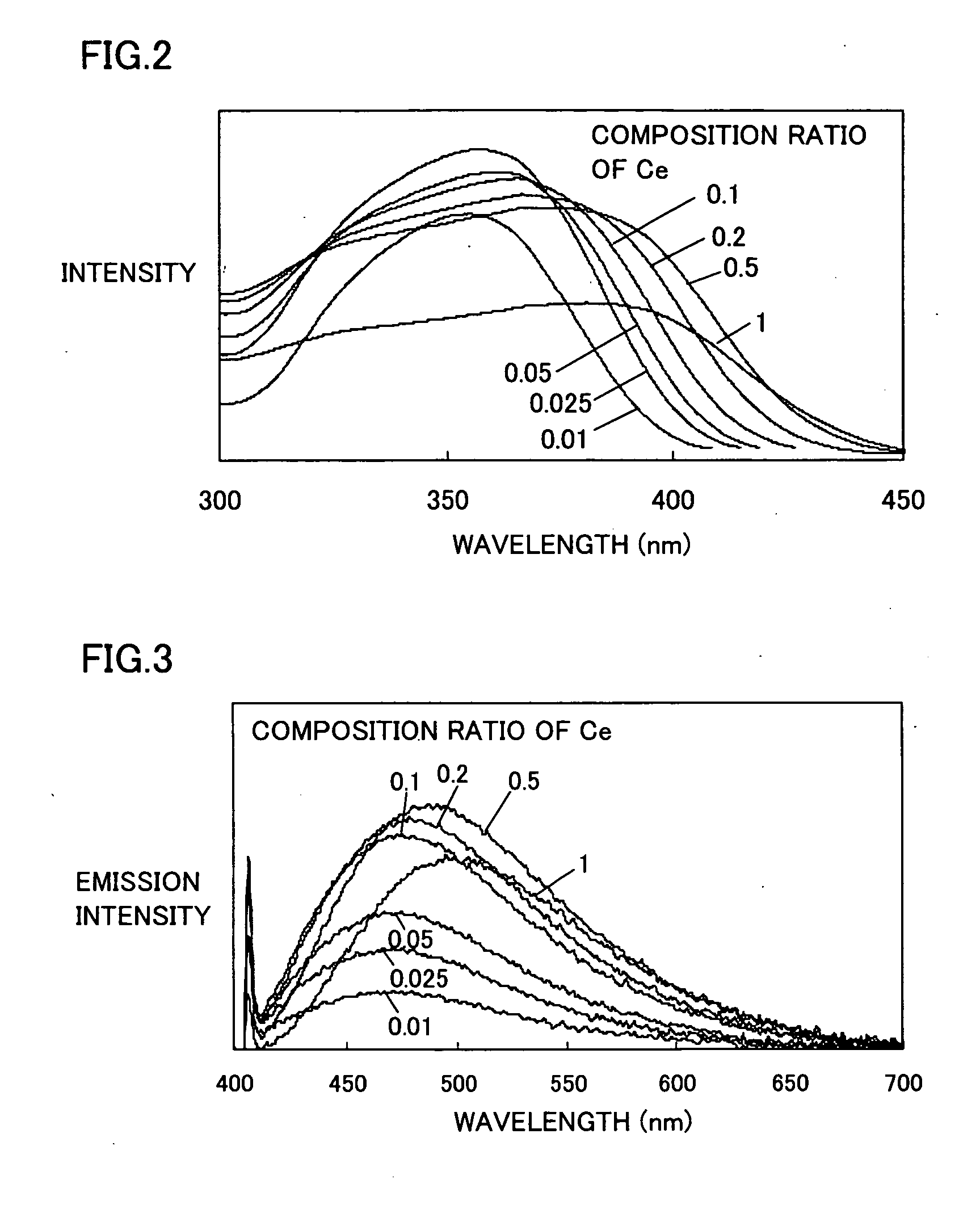
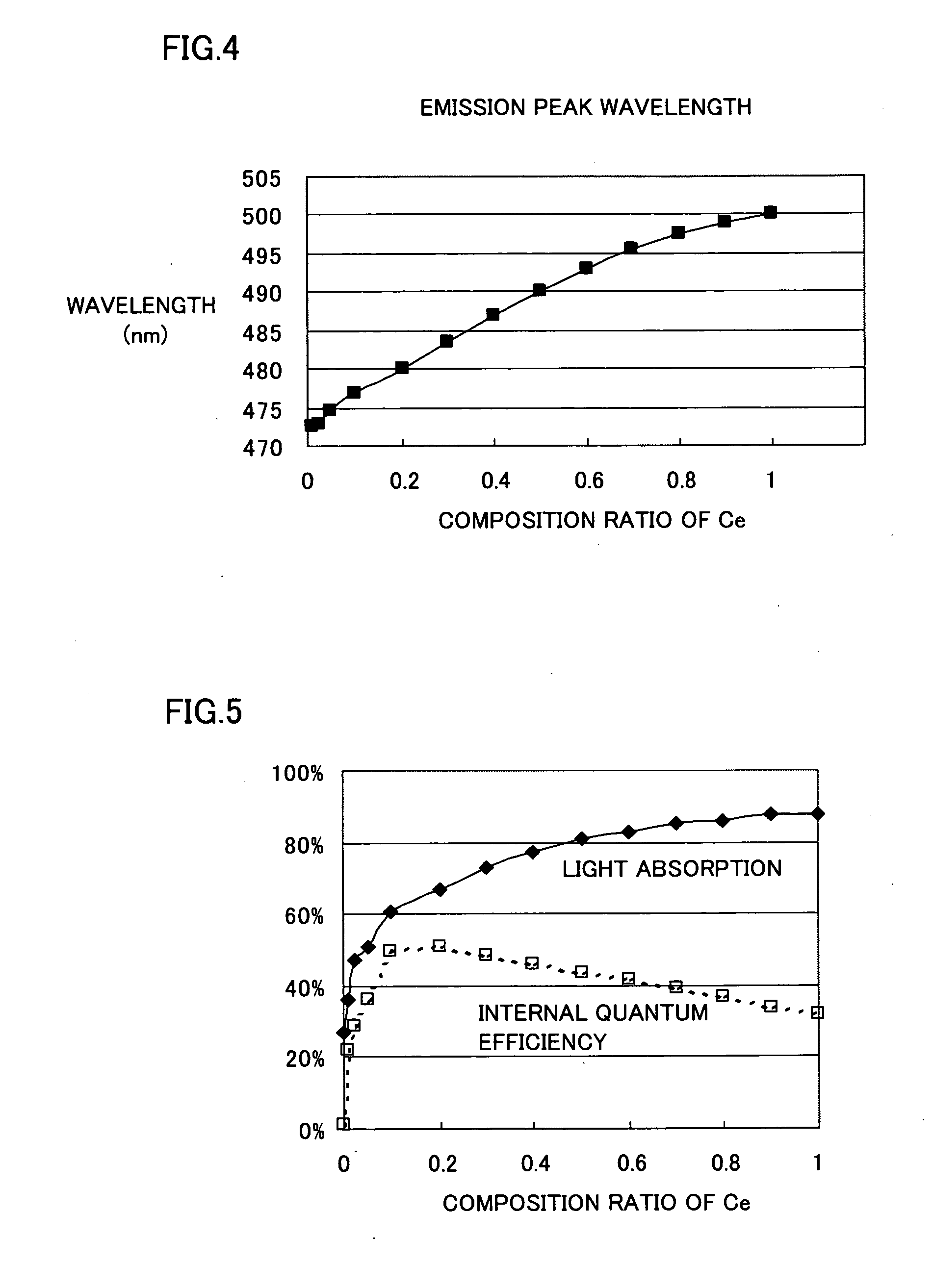
[0066] Ten kinds of example samples of which composition formula is represented by La1-aCeaSi5Al2O1.5N8.7 and composition ratios a of Ce, respectively, are different in the range of 0.1≦a≦1 and four kinds of comparative example samples having separate composition ratios a of Ce were prepared as follows.

[0067] Silicon nitride powder having an average particle diameter of 0.5 μm, an oxygen content of 0.93 mass % and an α-type content of 92%, aluminum nitride powder, lanthanum oxide powder and cerium oxide powder were weighed so as to be material ratios (mass %) shown respectively in Table 2 and mixed. The mixed powder was put in a boron nitride crucible and the crucible was introduced in a graphite resistance heating electric furnace.

TABLE 2CompositionRaw material composition (percent by mole)ratio of CeSi3N4La2O3CeO2AlNExample 10.148.74730.573.5917.09Example 20.248.65327.127.1617.06Example 30.348.5623.6910.717.03Example 40.448.46720.2614.317.00Example 50.548.37416.8517.816.96Examp...

example 11

[0079] In the next place, an example of a semiconductor light-emitting device according to the invention, which uses an oxynitride phosphor according to Example 3 and has high brightness, will be described.

[0080]FIG. 9 is a sectional view showing a semiconductor light-emitting device according to Example 11 of the invention. The semiconductor light-emitting device shown in FIG. 9 has a semiconductor light-emitting element 7 that has an InGaN layer as an active layer and an emission peak wavelength at 405 nm disposed on a printed wiring board 8 as a substrate. Inside of a resin frame 9, a mold resin 3 made of a transparent epoxy resin in which a phosphor is dispersed is filled to seal the semiconductor light-emitting element 7. Inside of the resin frame 9, one electrode portion 8a on the printed wiring board 8 and an N side electrode 5 on a bottom surface of the semiconductor light-emitting element 7 are adhered with an adhesive 15 having the electrical conductivity to electrically ...

example 12

[0083] In the next place, another example of a bright semiconductor light-emitting device that uses the oxynitride phosphor prepared according to Example 6 will be explained.

[0084] A sectional structure of the semiconductor light-emitting device according to the example has a structure similar to that of FIG. 9. Similarly, in order to obtain white emission color, three kinds of phosphors below were blended and dispersed in a mold resin. In the example, a first phosphor (emission peak wavelength: 484 nm) made of an oxynitride phosphor that is represented by a composition formula La0.4Ce0.6Si5Al2O1.5N8.7 according to Example 6 and has blue emission as a main emission peak, a second phosphor (emission peak wavelength: 655 nm) that is represented by a formula CaAlSiN3: Eu2+ and has a red emission as a main emission peak and a third phosphor (emission peak wavelength: 537 nm) that is represented by a formula β-sialon: Eu2+ and has a green emission as a main emission peak were blended an...


PUM

PropertyMeasurementUnit
emission peak wavelengthaaaaaaaaaa

Abstract

The invention provides an oxynitride phosphor represented by a composition formula M1-aCeaSibAlcOdNe, wherein M denotes La or a compound of which main component is La and sub-component is at least one kind of element selected from the group consisting of Pr, Nd, Sm, Eu, Gd, Th, Dy, Ho, Er, Tm, Yb and Lu; the a that represents a composition ratio of Ce is a real number satisfying 0.1≦a≦1; the b that represents a composition ratio of Si is a real number satisfying b=(6−z)×f; the c that represents a composition ratio of Al is a real number satisfying c=(1+z)×g; the d that represents a composition ratio of O is a real number satisfying d=z×h; the e that represents a composition ratio of N is a real number satisfying e=(10−z)×i; the z is a real number satisfying 0.1≦z≦3; the f is a real number satisfying 0.7≦f≦1.3; the g is a real number satisfying 0.7≦g≦3; the h is a real number satisfying 0.7≦h≦3; the i is a real number satisfying 0.7≦i≦1.3; and a JEM phase is contained in an amount of 50% or more, and a semiconductor light-emitting device that uses the oxynitride phosphor.

Description

[0001] This nonprovisional application is based on Japanese Patent Application No. 2005-045009 filed with the Japan Patent Office on Feb. 22, 2005, the entire contents of which are hereby incorporated by reference. BACKGROUND OF THE INVENTION [0002] 1. Field of the Invention [0003] The present invention relates to an oxynitride phosphor that has a JEM phase as a main component and a semiconductor light-emitting device using the oxynitride phosphor. Specifically, the invention relates to a semiconductor light-emitting device that can be used for a backlight light source for liquid crystal displays, a portable telephone, a portable information terminal, an LED (light-emitting diode) display device used for indoor and outdoor advertisements, an indicator for various kinds of portable units, or a light source for an illumination switch or OA (office automation) units. The invention particularly relates to a semiconductor light-emitting device where an oxynitride phosphor converts an wav...

Claims


Application Information

Patent Timeline
Patent Type & Authority Applications(United States)
IPC IPC(8): H01L33/00H01J1/62C09K11/08H01L33/32H01L33/50H01L33/56H01L33/62
CPCC09K11/7774H01L33/502H01L2224/48091H01L2224/48465H01L2224/73265H01L2924/00014H01L2924/00C09K11/77748
Inventor TAKAHASHI, KOHSEIHIROSAKI, NAOTO
Owner SHARP KK
Why Eureka
Try Eureka