Crystallization method, crystallization apparatus, processed substrate, thin film transistor and display apparatus

a crystallization apparatus and substrate technology, applied in the direction of crystal growth process, manufacturing tools, instruments, etc., can solve the problems of reducing the thickness of the substrate plate, the inability of the transistor to be suitable for the display apparatus, and the inability to optimize the light intensity distribution

Inactive Publication Date: 2006-08-24
SHARP KK
View PDF3 Cites 20 Cited by
  • Summary
  • Abstract
  • Description
  • Claims
  • Application Information

AI Technical Summary

Benefits of technology

[0096]FIG. 27 is a type drawing illustrating an effect of the present invention;
[

Problems solved by technology

Irregularities are generated in characteristics of each thin film transistor due to nonuniformity in the number of crystal grain boundaries and, in particular, there is a problem that this transistor is not suitable for a display apparatus which requires uniform display in one screen.
However, when the silicon film is crystallized by using the conventi

Method used


Image

  • Crystallization method, crystallization apparatus, processed substrate, thin film transistor and display apparatus
  • Crystallization method, crystallization apparatus, processed substrate, thin film transistor and display apparatus
  • Crystallization method, crystallization apparatus, processed substrate, thin film transistor and display apparatus

Examples


Embodiment Construction

[0107] Embodiments according to the present invention will now be described hereinafter with reference to the accompanying drawings.

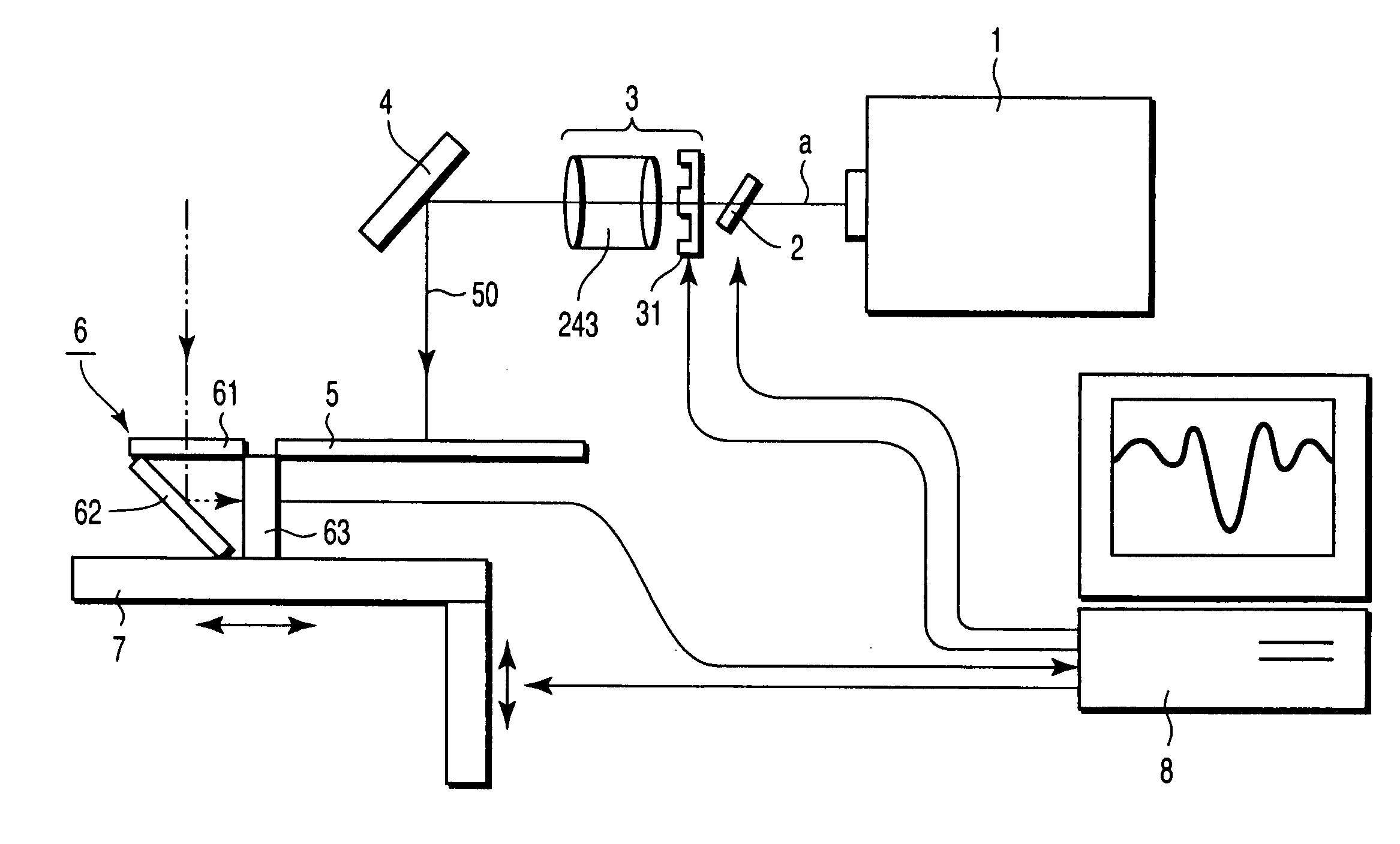
[0108]FIG. 1 is a schematic view showing a laser crystallization apparatus embodying the present invention. In a laser crystallization apparatus, an attenuator 2 and a beam profile modulation portion 3 are arranged at a starting end of an optical axis a of a laser beam source 1 containing the homogenization optical system, and a semiconductor substrate 5 is provided at a trailing end through a mirror 4. Further, a beam profile measurement portion 6 is provided to be aligned with the semiconductor substrate 5, and the semiconductor substrate 5 and the beam profile measurement portion 6 are fixed to a moving stage 7.

[0109] Furthermore, a control personal computer 8 as a controller is set, the beam profile measurement portion 6 is connected on an input side of the personal computer 8, and control systems of the attenuator 2, the beam profile modulation p...


PUM

PropertyMeasurementUnit
Thicknessaaaaaaaaaa
Thicknessaaaaaaaaaa
Lightaaaaaaaaaa

Abstract

There are provided a crystallization method which can design laser beam having a light intensity and a distribution optimized on an incident surface of a substrate, form a desired crystallized structure while suppressing generation of any other undesirable structure area and satisfy a demand for low-temperature processing, a crystallization apparatus, a thin film transistor and a display apparatus. When crystallizing a non-single-crystal semiconductor thin film by irradiating laser beam thereto, irradiation light beam to the non-single-crystal semiconductor thin film have a light intensity with a light intensity distribution which cyclically repeats a monotonous increase and a monotonous decrease and a light intensity which melts the non-single-crystal semiconductor. Further, at least a silicon oxide film is provided on a laser beam incident surface of the non-single-crystal semiconductor film.

Description

CROSS-REFERENCE TO RELATED APPLICATIONS [0001] This application is based upon and claims the benefit of priority from prior Japanese Patent Applications No. 2003-189093, filed Jun. 30, 2003; No. 2003-193779, filed Jul. 8, 2003; No. 2003-308935, filed Sep. 1, 2003; No. 2.003-402197, filed Dec. 1, 2003; and No. 2004-093200, filed Mar. 26, 2004, the entire contents of all of which are incorporated herein by reference. BACKGROUND OF THE INVENTION [0002] 1. Field of the Invention [0003] The present application relates to a technique to manufacture a field effect transistor at a surface layer part of a non-single-crystal semiconductor thin film, and to single-crystal or polycrystal semiconductor thin film substrate used to manufacture a field effect transistor, and to crystallization method, a crystallization apparatus, a thin film transistor and a display apparatus suitable for manufacture of a display apparatus such as a liquid crystal or an organic EL or an electronic apparatus such as...

Claims


Application Information

Patent Timeline
IPC IPC(8): H01L29/76G02F1/136B23K26/06C30B13/24H01L21/20H01L21/336H01L21/77H01L21/84H01L29/786
CPCB23K26/063B23K26/0639B23K26/0648C30B13/24H01L21/2026B23K26/0656H01L29/78675H01L27/1285Y10T117/1008Y10T117/1004H01L29/66757B23K26/064B23K26/0622B23K26/066H01L21/02686H01L21/02488H01L21/02422H01L21/02678H01L21/02532H01L21/0242H01L21/02595H01L21/02691G02F1/136
Inventor JYUMONJI, MASAYUKIOGAWA, HIROYUKIMATSUMURA, MASAKIYOHIRAMATSU, MASATOKIMURA, YOSHINOBUTANIGUCHI, YUKIOKATO, TOMOYA
Owner SHARP KK
Why Eureka
Try Eureka