Electrooptical devices, electrooptical thin crystal films and methods making same

a thin crystal film and electrooptical technology, applied in the field of electrooptical thin crystal films and methods making same, can solve the problems of low operation speed, current-induced heating of the p-n junction, complex manufacturing process of thin lithium niobate layers, etc., and achieve the effect of eliminating the disadvantages inheren

Inactive Publication Date: 2006-09-14
NITTO DENKO CORP
View PDF16 Cites 18 Cited by
  • Summary
  • Abstract
  • Description
  • Claims
  • Application Information

AI Technical Summary

Benefits of technology

[0022] Accordingly, it is an object of the present invention to provide an electrooptical device that eliminates the disadvantages inherent in the known devices described above.
[0026] A still further object of the present invention is to provide a low-cost, material-and-energy-saving method for producing electrooptical devices.
[0028] A further object of the present invention is to provide an electrooptical device that can obtain electrooptical effects without passing electric current through the layer of an electrooptical material.

Problems solved by technology

One disadvantage of the light modulator described above is that the manufacturing process for thin lithium niobate layers is very complicated.
One disadvantage of this device is the relatively low operation speed determined by the slow response of the liquid crystal.
One disadvantage of this type of light modulators is the current-induced heating of the p-n junction, which requires taking special measures to thermally stabilize the entire device.
Another disadvantage is the limitation imposed on the modulation frequency by the mechanism of light modulation employed in this device.
Indeed, the lifetime of the minority carriers injected through the p-n junction is limited, usually to about 10−6 seconds for the holes.
This requirement poses limitations on the system dimensions.
A further disadvantage related to the electric current passage is the large energy consumption, which increases with the current value.
One disadvantage of the ferroelectric ceramics is that they retain orientation of the domain polarization vector for an arbitrarily long time after switching off the film.
This property of the ferroelectric ceramics complicates the control system of the electrooptical devices.
Another disadvantage of the ferroelectric ceramics is the difficulty of ensuring a fast operation speed.
This fact and the delayed electrooptical response in such materials are related to the energy consumption for the formation and reorientation of the domain walls.
Additional disadvantage is the fatigue inherent in the ferroelectric ceramic materials.
Straining a ceramic material in the range corresponding to the spatial modulation of light (e.g., at the expense of partial repolarization) encounters difficulties related to the deformation character of the field-induced polarization.
Another disadvantage of the above device is extremely strong temperature dependence of the characteristics of a ferroelectric layer.
In order to exclude the temperature drift, it is necessary to provide the control device with a thermal stabilization system, which increases the energy consumption, complicates the device, and increases the cost of production.
A significant disadvantage of the device employing ferroelectric ceramics is the probability of phase distortions introduced into the data processed as a result of strong deformation of the ceramic plate and the inverse piezoelectric effect.
The presence of defects and internal stresses leads to degradation of the properties of such materials which are extremely sensitive to manufacturing process parameters, making production of the devices a difficult task.
However, optical devices employing liquid-crystalline molecular compounds possess a number of disadvantages, in particular, require specially prepared substrates, alignment layers, or high-vacuum conditions for the obtaining of highly ordered and clean structures.
Special and advanced technologies are employed and even these often cannot ensure the obtaining of films possessing a certain type of order and ensuring required optical anisotropy.
This absorption in the dye is related to the fact that the electric field of the light polarized parallel to the long axis of the dye molecules drives electrons to oscillate between the ends of the molecule, thus consuming the beam energy.
One disadvantage of the above optical device is the relatively low operation speed of, which is characterized by a switching time on the order of 0.1 second.
This device operates poorly at reduced temperatures, under which conditions the operation speed further sharply reduces.
The device has insufficient working life, which amounts to about 104 hours.

Method used


Image

  • Electrooptical devices, electrooptical thin crystal films and methods making same
  • Electrooptical devices, electrooptical thin crystal films and methods making same
  • Electrooptical devices, electrooptical thin crystal films and methods making same

Examples


example 1

[0109] This example illustrates the manufacture of an electrooptical anisotropic thin crystal film of a lyotropic liquid crystal based on sulfided indanthrone organic dye.

[0110] The films were prepared from a 9.5% aqueous solution of sulfided indanthrone capable of forming a hexagonal phase at room temperature. This organic dye occurred in the solution in the form of anisometric supramolecular complexes, which formed the basis of a crystal structure of the target film. The initial paste was applied onto a clean silicon or glass substrate by means of casting and spreading. Then the colloid system was treated to reduce the viscosity for the subsequent alignment step. The resulting solution formed a nematic phase or a mixture of nematic and hexagonal phases with a viscosity reduced from 1780 to 250 mPa / s. This preliminary conversion of the colloidal system into a high flow state is a first step before obtaining the high-quality anisotropic thin crystal films of the present invention. ...

example 2

[0114] This example illustrates the manufacture of electrooptical devices of the present invention.

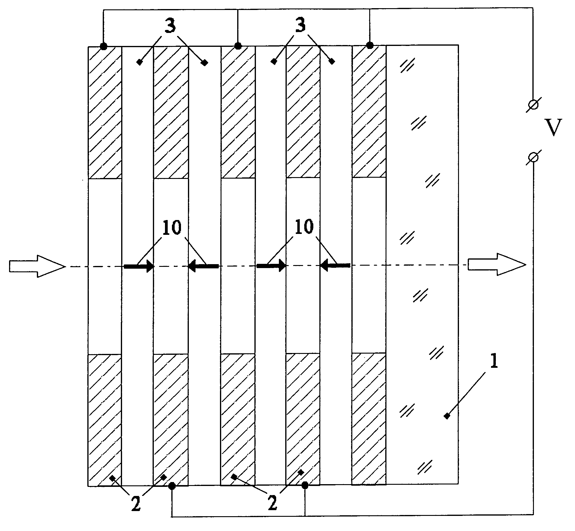
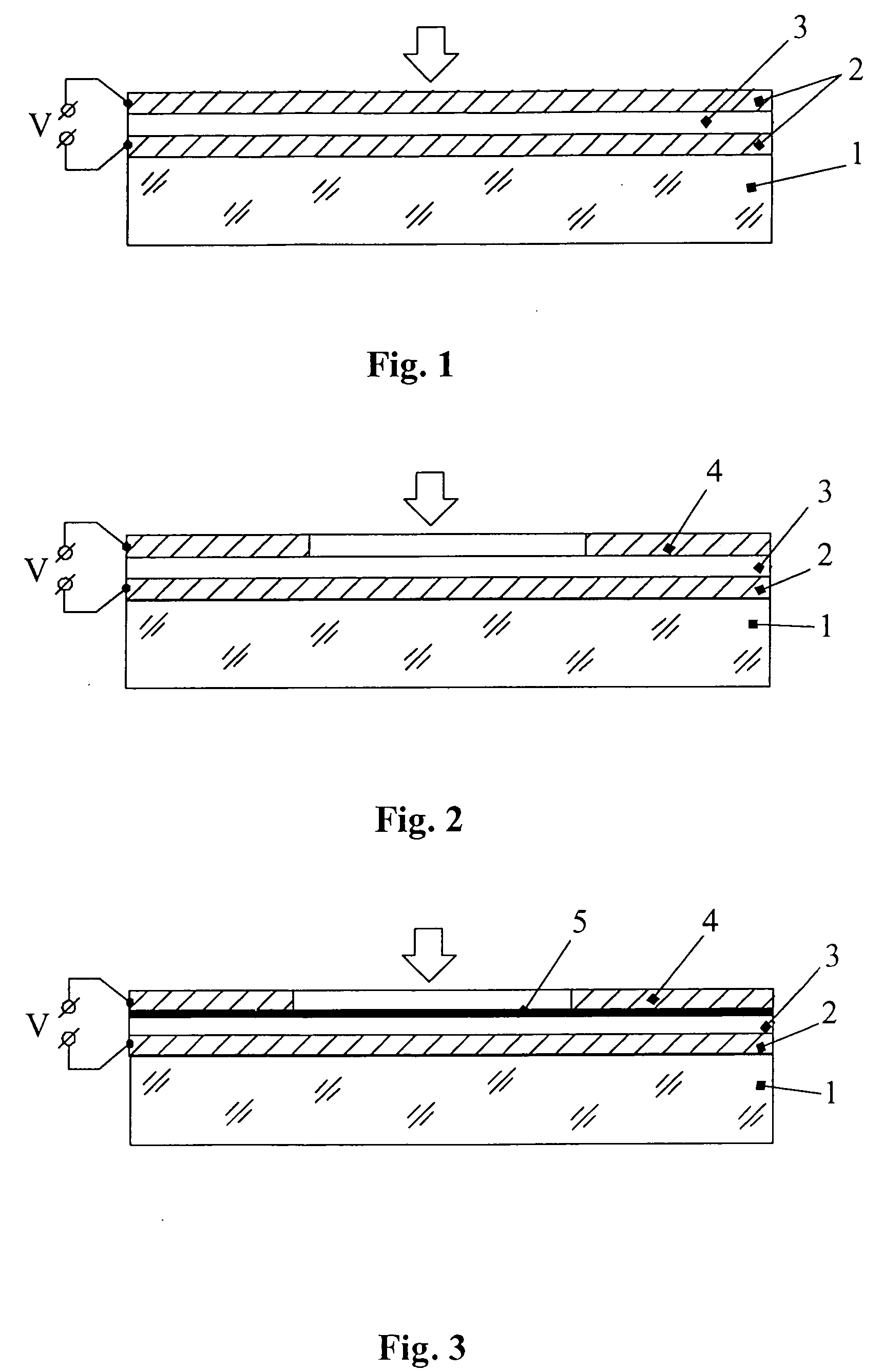
[0115] A layer of SnO2 with a thickness of 0.5 micron was formed by a conventional method. Above this film, an electrooptical anisotropic thin crystal film was formed according to the above described method, which was filled by a protective acetate film with a thickness of 10-20 nm. Then aluminum strips of four millimeter wide were deposited in vacuum onto the acetate film surface. Finally, the electrodes were attached and connected to a source of dc and / or ac control voltage.

example 3

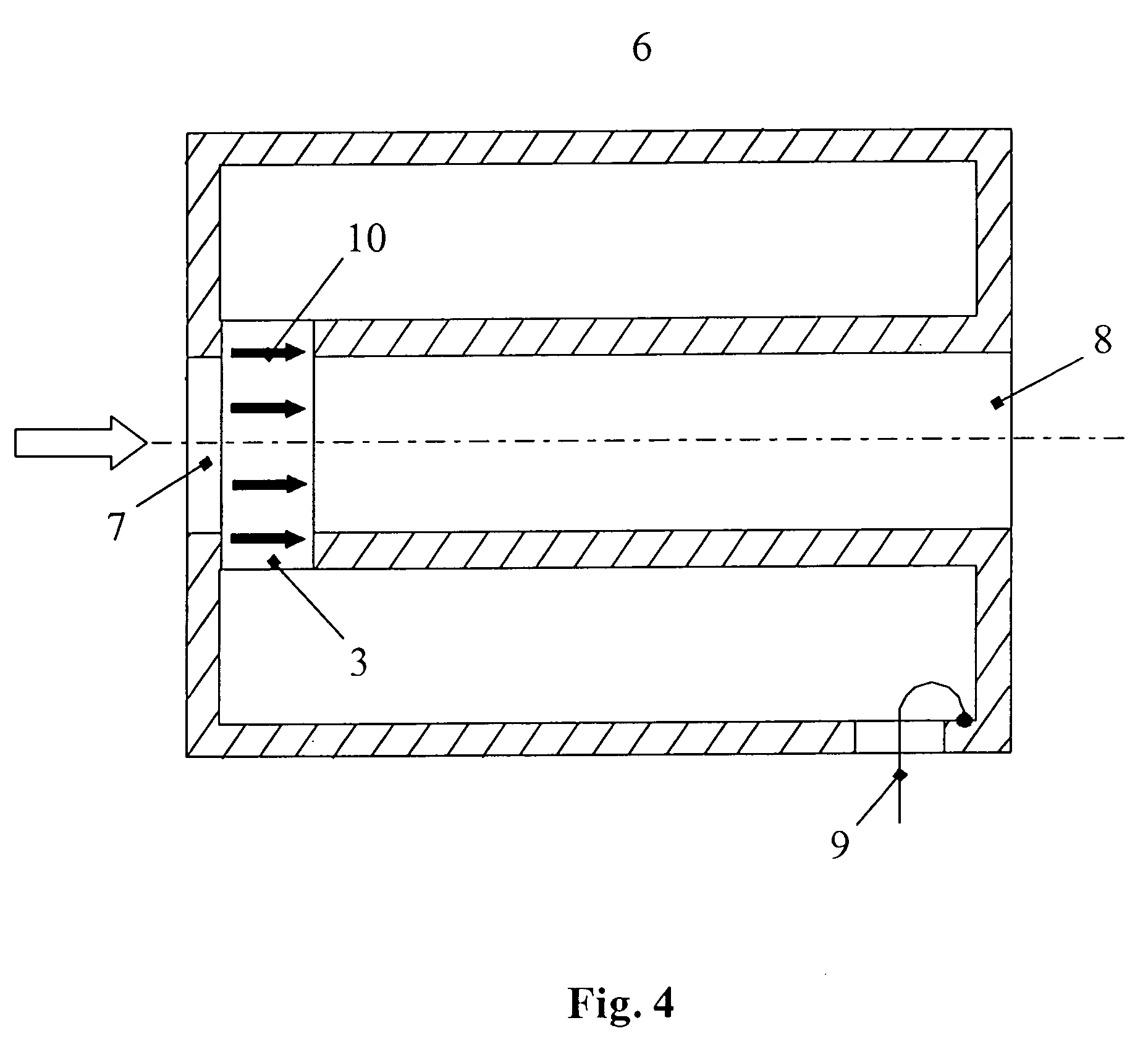
[0116] This example illustrates the manufacture of an electrooptical device based on a D-shaped optical fiber

[0117] A metal film was deposited on the flat surface of a D-shaped optical fiber. Then a gap of about five to ten micron wide was formed by a laser beam to divide the metal layer into two electrodes. Finally, an electrooptical anisotropic thin crystal film was formed above this multilayer structure according to the above described method.

[0118] Of advantages, the electrooptical devices of the present invention is capable of controlling radiation in the visible and near IR range. The electrooptical devices of the invention comprises layers of materials with variable refractive indices and / or absorption coefficients dependent on the strength of an applied electric field and / or the electric field component of visible or IR radiation. The electrooptical materials used in the present invention possess a number of useful properties including linear variation of the refractive in...


PUM

PropertyMeasurementUnit
humidityaaaaaaaaaa
thicknessaaaaaaaaaa
voltageaaaaaaaaaa

Abstract

A method of fabrication of an electrooptical device comprises depositing a colloid system of anisometric particles onto at least one electrode and / or onto at least one substrate and / or onto at least one layer of an isotropic or anisotropic material to form at least one layer of an electrooptical material, externally aligning the colloid system to form a preferred alignment of the colloid system particles, drying the colloid system, and forming at least one electrode and / or at least one layer of an isotropic or anisotropic material on at least a portion of the layer of the electrooptical material.

Description

FIELD OF THE INVENTION [0001] This invention relates in general to electrooptical devices, and particularly to electrooptical devices capable of controlling radiation in the visible and near IR range. BACKGROUND OF THE INVENTION [0002] Electrooptical devices based on electrooptical materials such as lithium niobate (LiNbO3), KDP and KTP have been hereto described. See I. P. Kaminov et al., “Optical Fiber Telecommunications”, Vol. IIIB, Ed. by Academic Press (1997). [0003] There are known electrooptical devices such as light modulators based on a D-shaped optical fiber and using a lithium niobate crystal. See W. Johnstone et al., “Fiber Optic Modulators Using Active Multimode Waveguide Overlays”, Electron. Lett., Vol. 27, No. 11, 894-896 (1991). D-shaped optical fiber, also called side-polished optical fiber, refers to an optical fiber having a D-shaped cross section. Light modulators of this type are usually produced on a plane-parallel plate of a quartz glass which is provided with...

Claims


Application Information

Patent Timeline
Patent Type & Authority Applications(United States)
IPC IPC(8): G02F1/00G02F1/035G02F1/01G02F1/061G02F1/065G02F1/1333G02F1/313
CPCG02F1/0118G02F1/035G02F1/0356G02F1/065G02F1/1326G02F1/3131G02F1/3132G02F2201/15G02F2201/302G02F2203/026
Inventor LAZAREV, PAVEL I.PAUKSHTO, MICHAEL V.SULIMOV, VLADIMIR
Owner NITTO DENKO CORP
Why Eureka
Try Eureka