Method and device for plasma-etching organic material film

a technology of organic material and plasma etching, which is applied in the direction of plasma technique, solid-state device details, semiconductor/solid-state device details, etc., can solve the problems of deterioration in the etching selectivity of organic material relative to inorganic material film, inability to achieve high etching rate and high etching selectivity simultaneously, disadvantageous in terms of considerably degraded uniformity in electron density (plasma density), etc., to achieve high selectivity and high uniform

Active Publication Date: 2006-09-28
KIOXIA CORP +1
View PDF6 Cites 31 Cited by
  • Summary
  • Abstract
  • Description
  • Claims
  • Application Information

AI Technical Summary

Benefits of technology

[0006] The present invention has been made in view of the above context. An object of the present invention is to provide a method and apparatus for plasma-etching an organ

Problems solved by technology

Thus, a facet formation of an inorganic material film, which is disposed adjacent to the organic material film to serve as a mask, is damaged by drawn ions, resulting in a deterioration in etching selectivity of the organic material film relative to the inorganic material film.
Namely, a high etching rate and a high etching selectivity cannot be simultaneously attained.
This method is, h

Method used


Image

  • Method and device for plasma-etching organic material film
  • Method and device for plasma-etching organic material film
  • Method and device for plasma-etching organic material film

Examples


Embodiment Construction

[0052] An embodiment of the present invention will be described below with reference to the accompanying drawings.

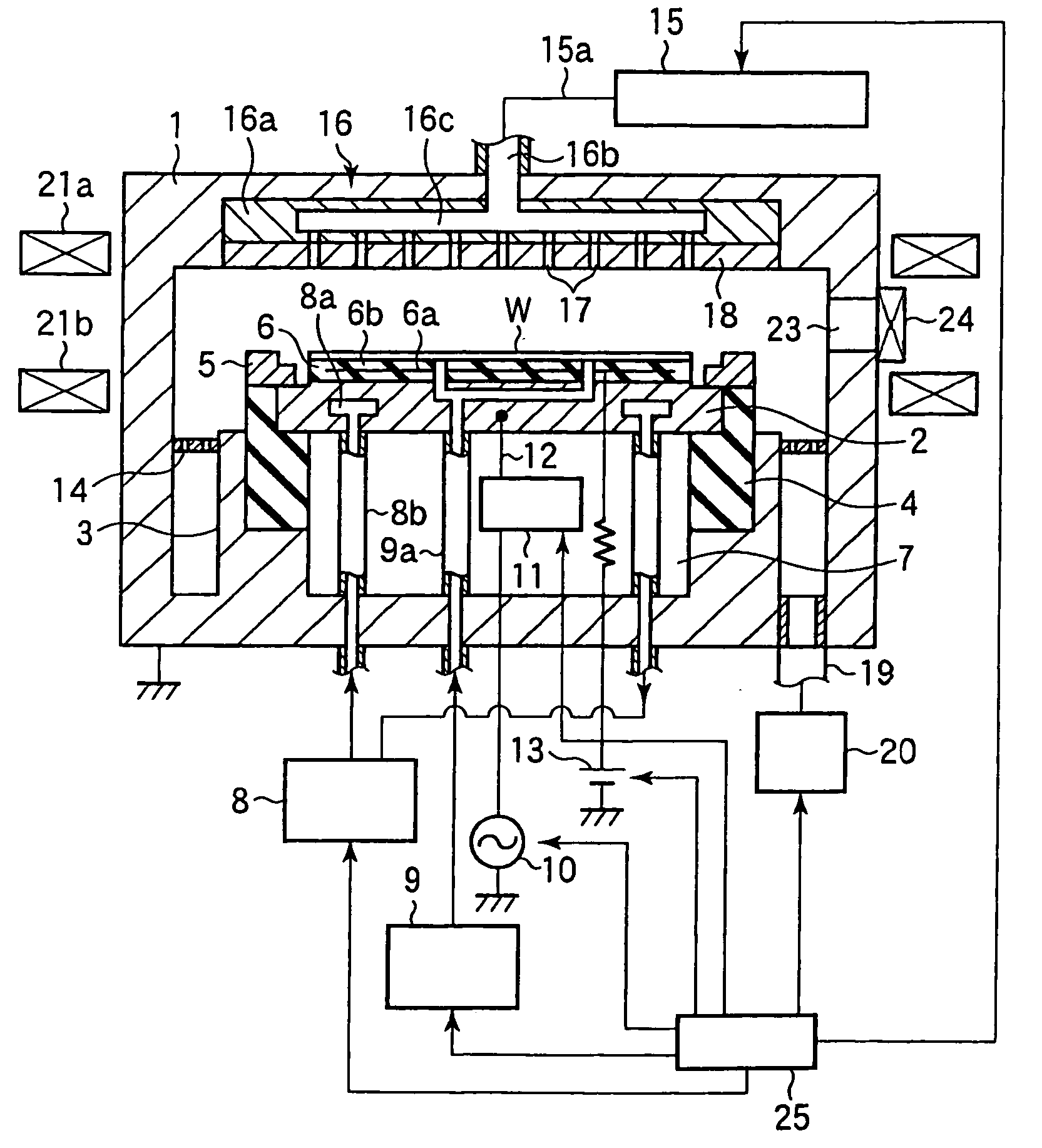
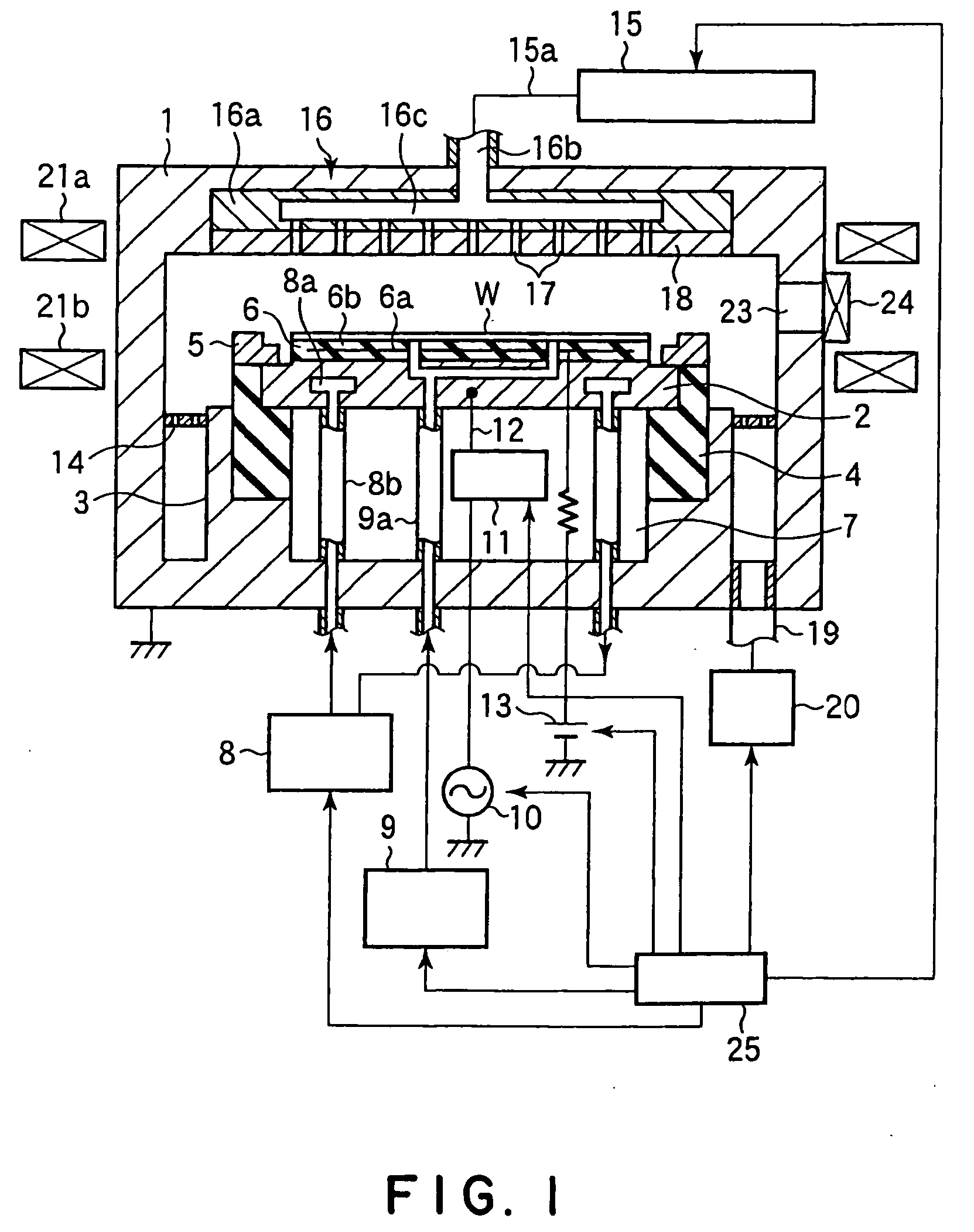
[0053]FIG. 1 is a sectional view of a plasma-etching apparatus for use in carrying out the present invention. The etching apparatus includes an air-tight, almost cylindrically-shaped process vessel 1 made of, e.g., aluminum. A wall surface of the process vessel 1 is oxidized. The process vessel 1 is grounded.

[0054] In the process vessel 1, there is disposed a support table 2 that horizontally supports a wafer W as a substrate, and serves as a support electrode (lower electrode). The table 2 is made of, e.g., aluminum and its surface is oxidized. The table 2 is supported by a support unit 3 projecting from a bottom wall of the process vessel 1 through an insulation member 4. A focus ring 5 made of a conductive material or insulative material is disposed to correspond to an upper periphery of the table 2. When a diameter of the wafer W is 300 mm+, the focus ring 5 having...


PUM

PropertyMeasurementUnit
Electric potential / voltageaaaaaaaaaa
Areaaaaaaaaaaa
Distanceaaaaaaaaaa

Abstract

A support electrode (2) and a counter electrode (16) constituting parallel plate electrodes are disposed in a process vessel (1). A substrate (W) with an organic material film formed thereon is supported by the support electrode (2). A high-frequency power of a frequency of 40 MHz or above for generating the plasma is applied to the support electrode (2), so that a high-frequency electric field is formed between the support electrode (2) and the counter electrode (16). A process gas is supplied into the process vessel (1) to generate plasma of the process gas by the high-frequency electric field. The organic material film on the substrate (W) is etched with the plasma, with an organic material film serving as a mask. The process gas includes an ionization accelerating gas, such as Ar, that is ionized from a ground state or metastable state with an ionization energy of 10 eV or below and has a maximum ionization cross-section of 2×1016 cm2 or above.

Description

FIELD OF THE INVENTION [0001] The present invention relates to a method and apparatus for plasma-etching an organic material film such as a low dielectric constant film (low-k film) formed on a substrate of a semiconductor wafer or the like. BACKGROUND ART [0002] In a wiring process of a semiconductor device, an interlayer dielectric film disposed between wiring layers is etched for conducting the wiring layers. In view of the recent demand for higher speed of a semiconductor device, an interlayer dielectric film has been required to have a lower dielectric constant, and an organic material film has been used as such a low dielectric constant film. [0003] An organic material film is etched with plasma, using an inorganic material film, such as silicon oxide, as a mask. To be specific, as disclosed in Japanese Patent Laid-Open Publications No. 2001-60582 and No. 2001-118825, the plasma-etching process is carried out by means of a plasma-etching apparatus, in which a pair of parallel ...

Claims


Application Information

Patent Timeline
IPC IPC(8): C23F1/00H01L21/306B44C1/22H01J37/32H05H1/46H01L21/3065H01L21/311H01L21/768H01L23/522
CPCH01J37/32522H01J37/32633H01L21/31138H01J37/32688H01J2237/3341H01J37/32642
Inventor HONDA, MASANOBUMATSUYAMA, SHOICHIRONAGASEKI, KAZUYAHAYASHI, HISATAKA
Owner KIOXIA CORP
Why Eureka
Try Eureka