Electronic and optical devices and methods of forming these devices

a technology of optical devices and electronic devices, applied in the direction of instruments, non-linear optics, optical elements, etc., can solve the problems of affecting the designability of radio frequency (rf) or electrooptic devices, affecting the freedom of designability of radio frequency or electrooptic devices, etc., to minimize the interaction with wave propagation, minimize loss, and minimize leakage

Inactive Publication Date: 2006-10-12
NGIMAT CO
View PDF5 Cites 16 Cited by
  • Summary
  • Abstract
  • Description
  • Claims
  • Application Information

AI Technical Summary

Benefits of technology

[0024] Any loss that is caused by the biasing electrodes is offset by the benefit to the system wherein the use of higher voltages as well as enabling the optimal, functional, device design including conductor separation. The materials of the biasing electrodes can be grown as a base layer (potentially epitaxial) prior to the variable dielectric material or they can be grown on top of the dielectric material or otherwise deposited thereon to form the system. To further minimize loss, the material can be discontinuous in design, so it is not a full sheet but has fine lines in various patterns. To further minimize the interaction with the wave propagation between the electrodes, the biasing electrodes can be formed as strips that are diagonal to the main electrodes (system lines), parallel to the system lines, or perpendicular to the system lines. The top and bottom bias strips can be directly across the thin film, or alternating. Alternating the bias strips will minimize leakage and can better align dielectric changes with some devices, but this can also slightly increase the bias voltage needed. The highly conductive main electrode device lines can be on one surface of the dielectric material film, with the bias voltage being applied between a main electrode that is electrically connected to one of the bias electrodes, and the biasing electrode on the other side of this thin film variable dielectric material. Alternatively, one device line can be contacting and used to apply the potential to one bias electrode and another device line can contact and be used to apply the potential to the other bias electrode thereby applying the net potential across the variable dielectric. Using the highly conductive device lines to apply the potential to shorter, more resistive bias electrodes will increase the speed of change in the variable dielectric, resulting in faster device speeds. The non-RF bias electrodes can also be deposited on only one surface and be formed as interdigital electrodes.
[0025] To further illustrate the advantage of the biasing electrodes of the present invention, we should consider the previous method of reducing the required tuning voltage for prior art tunable capacitors, wherein it is often necessary to reduce the gap between electrodes to very small values, so small voltages can result in large electric fields. However, this method of providing low voltage tuning, can induce distortions in the RF signal. For example, a critical problem for systems based on tunable capacitors is intermodulation distortion. The phenomenon of intermodulation distortion occurs when the amplitude of the RF signal is sufficiently high that the RF voltage itself can affect the value of the tunable capacitor itself. This induced nonlinearity can cause distortion of the RF signal.
[0026] In the present invention, the phenomenon of intermodulation distortion is addressed by increasing the gap between the RF electrodes, thereby reducing the intensity of the RF-induced fields in the ferroelectric materials, and maintaining the dielectric constant of the materials approximately invariant to RF field strength. However, the DC tuning voltage is maintained low by extending highly resistive protrusions of material into the space between the RF electrodes. These protrusions are preferentially electrically connected to the RF electrodes themselves. Since the ferroelectric material prese

Problems solved by technology

This results in a change of capacitance or electromagnetic wave transmission between two main terminals also attached or in close proximity to the variable material.
The device conductors are used versus adding additional conductors to apply the bias because additional traditional conductors would affect the device performance.
This creates a limit due to the dimensional tolerance

Method used


Image

  • Electronic and optical devices and methods of forming these devices
  • Electronic and optical devices and methods of forming these devices
  • Electronic and optical devices and methods of forming these devices

Examples


example 1

Deposition of BST on Sapphire

[0114] In this example, Ba0.6Sr0.4TiO3 coatings were deposited onto C-plane Sapphire 250 nanometers thick using the CCVD process. The solution of the Ba0.6Sr0.4TiO3 precursor contained 0.0143 wt % of Sr in the form of strontium 2-ethylhexanoate, 0.0615 wt % of Ba in the form of barium 2-ethylhexanoate, 0.0355 wt % Ti (di-1-propoxide)bis(acetylacetonate), 12.6049 wt % toluene, 0.0118 wt % isoproponal, 1.5333 wt % 1-butanol, and 85.7412 wt % propane. The constant flow rate for the solution was at 2.0 ml / min and for the tip oxygen 4000 ml / min at 80 psi. The gas temperature as measured close to the substrate front surface varied from 900 to 1100° C. BST deposition was epitaxial with 1,1,1 lattice structure.

example 2

[0115] Deposition of BST on Sapphire and Device Construction In this example, Ba0.6Sr0.4TiO3 coatings were deposited onto C-plane Sapphire 377 nanometers thick using the CCVD process. The solution of the Ba0.6Sr0.4TiO3 precursor contained 0.0143 wt % of Sr in the form of strontium 2-ethylhexanoate, 0.0615 wt % of Ba in the form of barium 2-ethylhexanoate, 0.0355 wt % Ti (di-1-propoxide)bis(acetylacetonate), 12.6049 wt % toluene, 0.0118 wt % isoproponal, 1.5333 wt % 1-butanol, and 85.7412 wt % propane. The constant flow rate for the solution was at 3.0 ml / min and for the tip oxygen 4000 ml / min at 80 psi. The gas temperature as measured close to the substrate front surface was 1200° C. Deposition was epitaxial with 1,1,1 lattice structure.

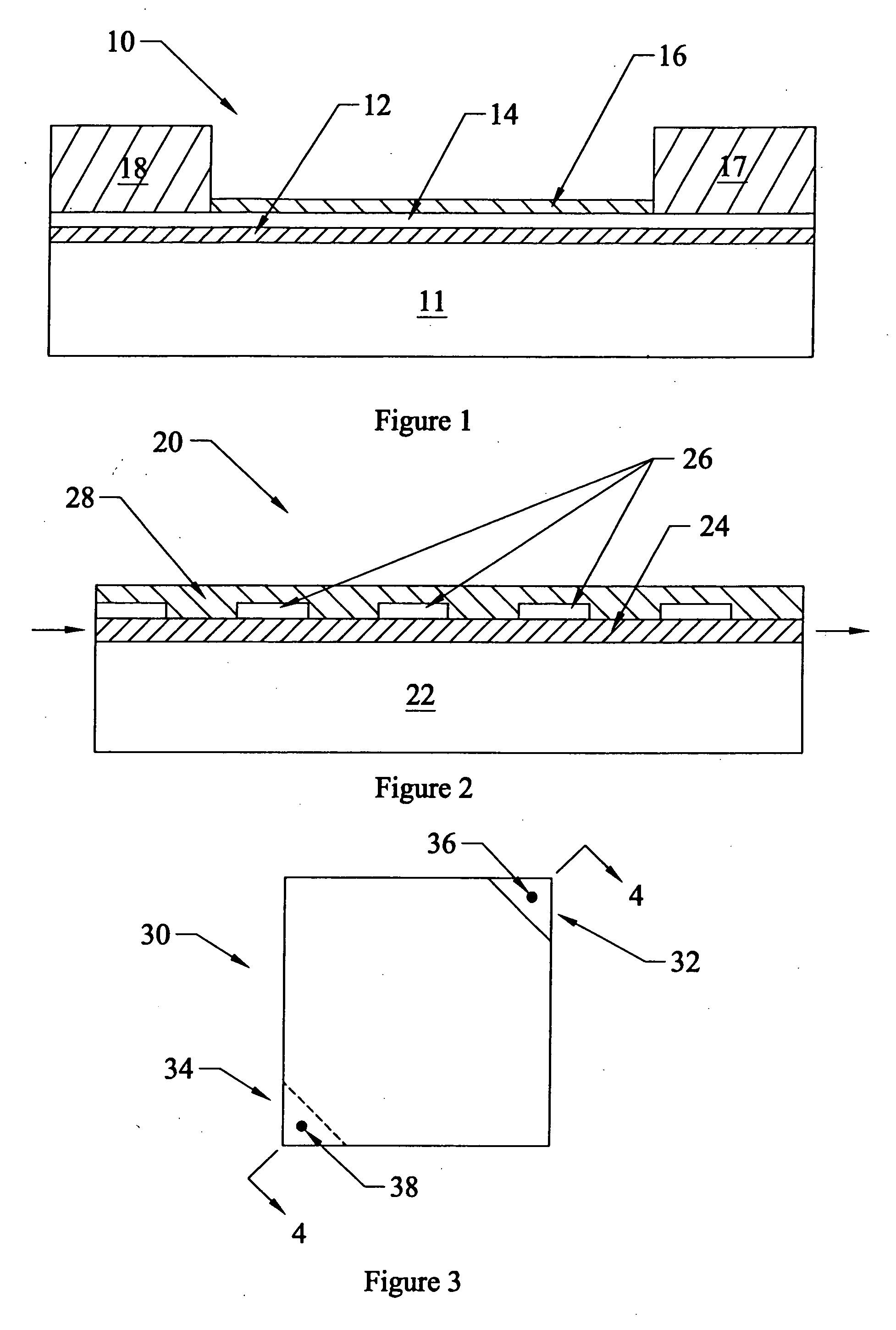
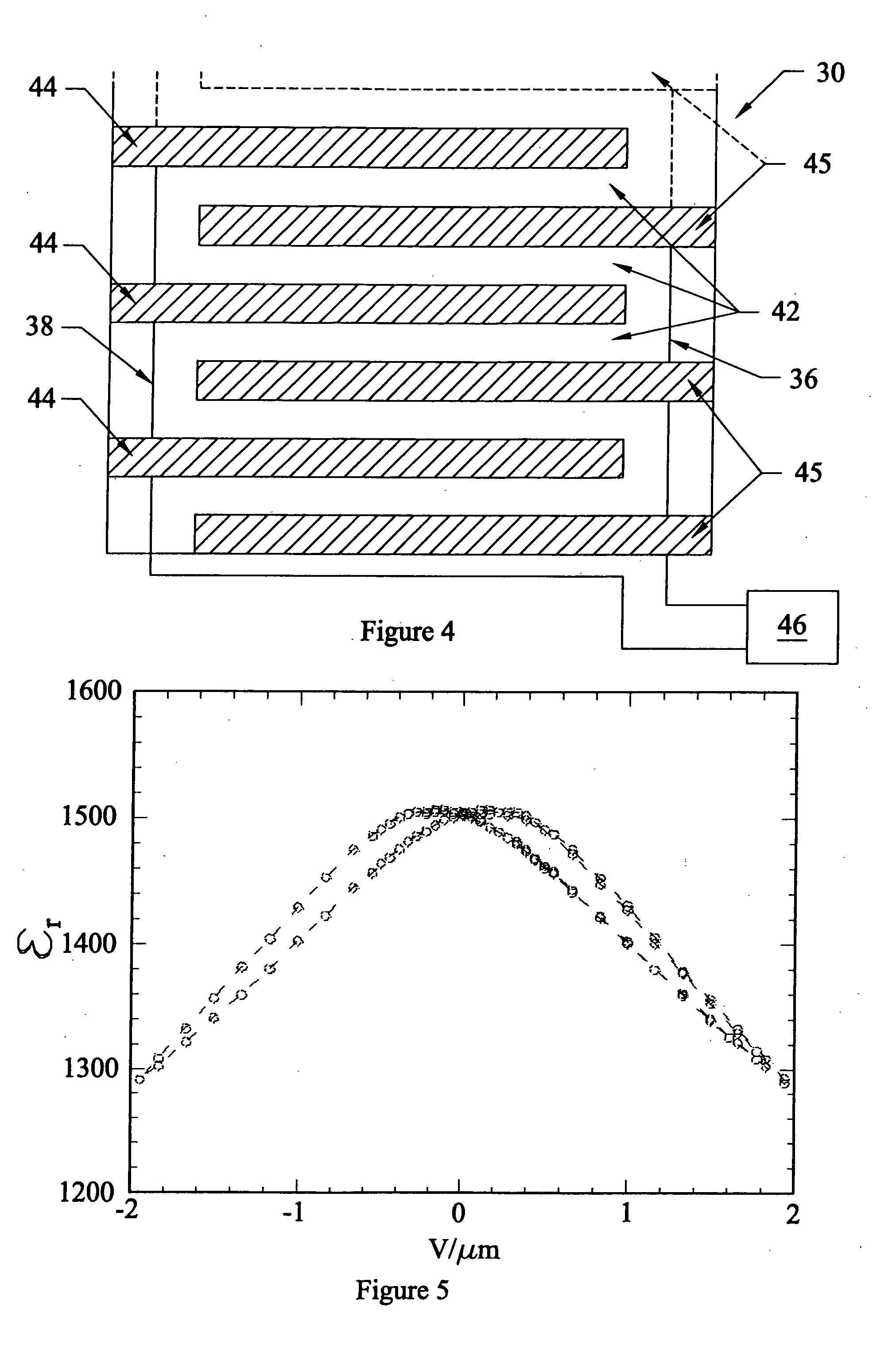
[0116] After forming the BST layer, a chromium bond layer and a gold conductive layer were formed on top of the BST using conventional coating methods. The chromium and gold were then patterned to form two electrodes of a 50 finger interdigital capa...

example 3

[0119] In this example, Ba0.6Sr0.4TiO3 coatings were deposited onto polycrystalline alumina using the CCVD process. Polycrystalline alumina is a less expensive substrate material, but prior art techniques to deposit BST on alumina have resulted in significantly lower performance. By using CCVD, a quality layer was formed. The solution of the Ba0.6Sr0.4TiO3 precursor contained 0.0143 wt % of Sr in the form of strontium 2-ethylhexanoate, 0.0615 wt % of Ba in the form of barium 2-ethylhexanoate, 0.0355 wt % Ti (di-i-propoxide)bis(acetylacetonate), 12.6049 wt % toluene, 0.0118 wt % isopropanol, 1.5333 wt % 1-butanol, and 85.7412 wt % propane. The constant flow rate for the solution was at 5.0 ml / min and for the tip oxygen 4020 ml / min at 30 psi. The gas temperature as measured close to the substrate front surface was 1150° C.


PUM


Abstract

Electronic and optical (or photonic) devices with variable or switchable properties and methods used to form these devices, are disclosed. More specifically, the present invention involves forming layers of conductive material and dielectric material or materials with varying conductivity and indexes of refraction to form various electronic and optical devices. One such layer of adjustable material is formed by depositing epitaxial or reduced grain boundary barium strontium titanate on the C-plane of sapphire.

Description

[0001] The present invention is directed to electronic and optical (or photonic) devices with variable or switchable properties and methods used to form these devices. More specifically, the present invention involves forming layers of conductive material and dielectric material or materials with varying conductivity and indexes of refraction to form various electronic and optical devices. BACKGROUND OF THE INVENTION [0002] Thin films (and thick films in some cases) are useful for forming many different electronic and optical devices. Capacitors (and other devices such as phase shifters) are formed by depositing dielectric material and conductive material layers, the conductive layer(s) forming the electrodes of the capacitor. In optical devices, films of material having relatively high indexes of refraction are deposited adjacent to films of materials having relatively low indexes of refraction to form wave-guides, filters, lenses and other devices. Many materials are useful for fo...

Claims


Application Information

Patent Timeline
IPC IPC(8): G02F1/035
CPCG02F1/0316G02F1/0508H01G7/06H01L29/93H01L27/016H01L27/13H01L21/86
Inventor HUNT, ANDREW T.SCHWERZEL, ROBERT E.JIANG, YONGDONGZHAO, ZHIYONGPOLLEY, TODD
Owner NGIMAT CO
Why Eureka
Try Eureka