Charged particle beam apparatus

a technology of charged particle beam and beam apparatus, which is applied in the direction of magnetic discharge control, nuclear engineering, therapy, etc., to achieve the effect of facilitating miniaturization and prolonging the time period over which high vacuum is maintained

Inactive Publication Date: 2006-10-19
HITACHI HIGH-TECH CORP
View PDF16 Cites 82 Cited by
  • Summary
  • Abstract
  • Description
  • Claims
  • Application Information

AI Technical Summary

Benefits of technology

[0014] The present invention is achieved by making an electron optical system of the charged particle beam apparatus have a differential pumping structure, placing a nonevaporative getter pump in a vacuum chamber on the upstream side, placing a minimum number of ion pumps in a vacuum chamber on the downstream side, and using both the pumps together. To the ion pump is more preferably applied a sputter ion pump pumping out a rare gas with high efficiency, or a noble ion pump. As a noticeable effect, a time period over which high vacuum is maintained can considerably be prolonged.
[0016] By using the present invention, small-sized charged particle beam apparatuses capable of maintaining the inside of a column under high vacuum of an order of 10−8 Pa, for example a small-sized scanning electron microscope, a focused ion beam apparatus and a charged particle beam apparatus having a plurality of columns can be obtained. By applying the present invention to a magnetic-field-superposed electron gun, miniaturization can be facilitated, and a time period over which high vacuum is maintained can considerably be prolonged.
[0017] Further, a small-sized SEM column for monitoring a position of a probe of a prober apparatus directly measuring an electric property of a semiconductor can be easily included.
[0018] As another effect, an electron beam irradiation column of a mirror projection type electron beam inspection apparatus for inspection of semiconductor elements can be miniaturized.

Problems solved by technology

Further, another problem is solved by mounting a detachable coil or permanent magnet on an electron gun part.

Method used


Image

  • Charged particle beam apparatus
  • Charged particle beam apparatus
  • Charged particle beam apparatus

Examples


embodiment 1

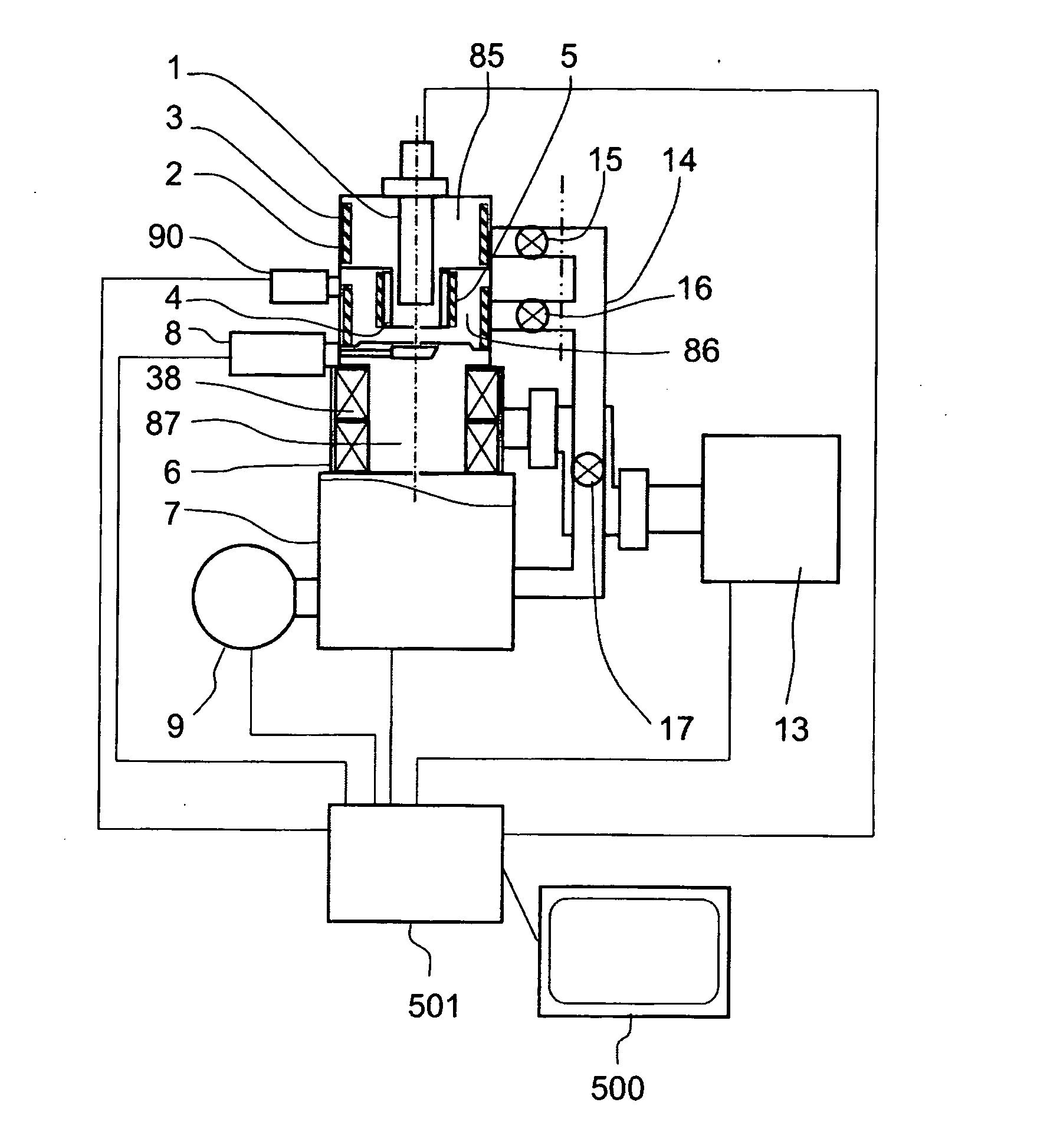
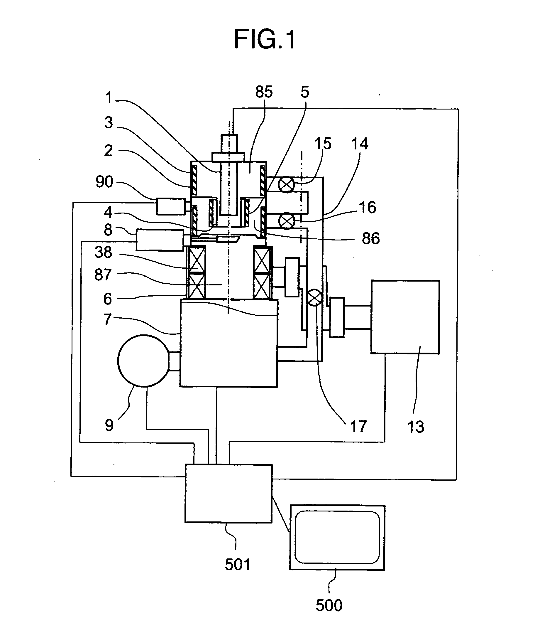
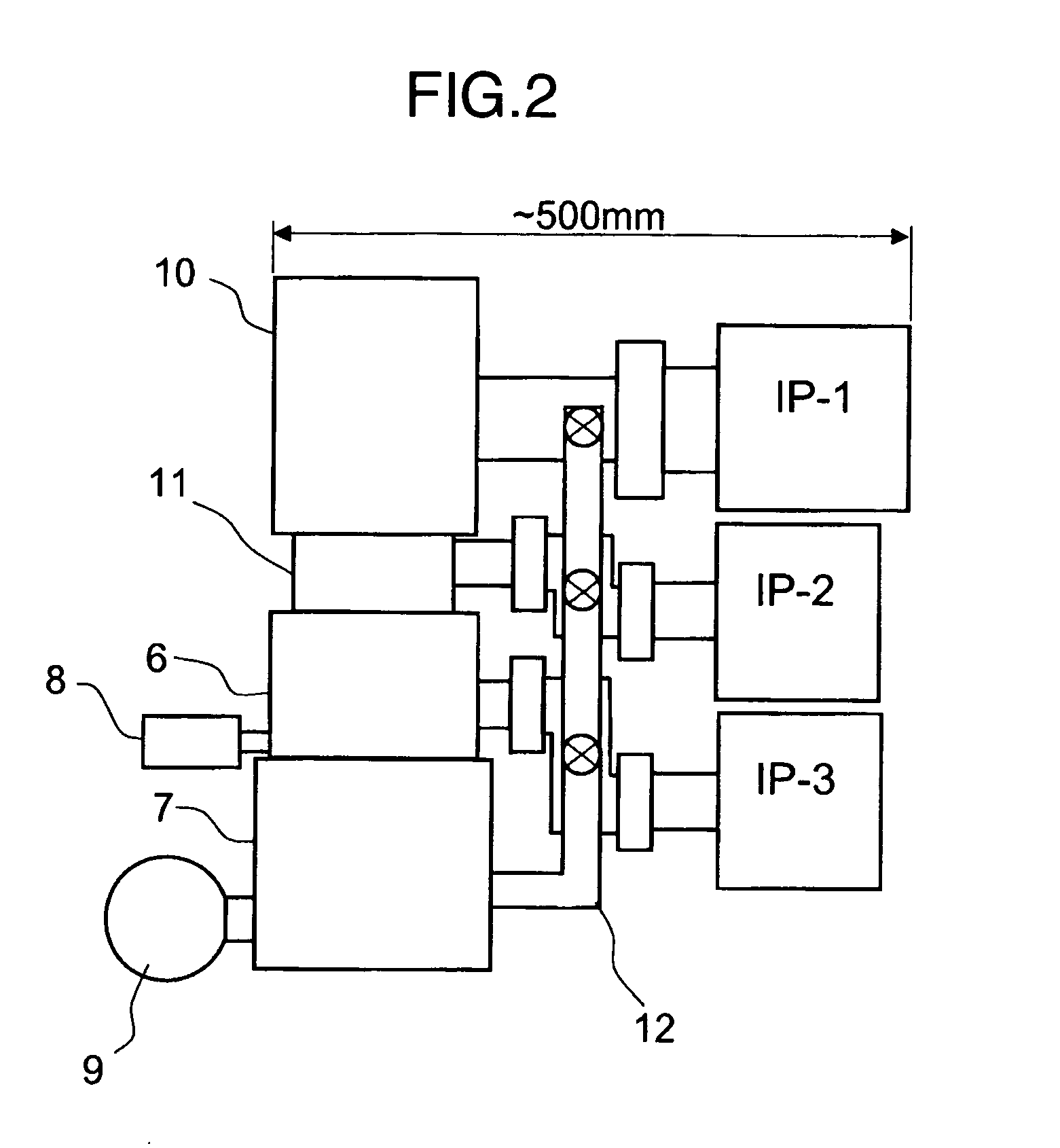
[0042]FIG. 1 shows an embodiment according to the present invention. As an electron source, a thermal field emitter (TFE) is used. This electron source 1 is mounted on the flange of 152 mm in diameter and is combined with a feedthrough to electrodes (suppressor, extractor electrode and chip) not shown in the drawing. This electron source 1 is inserted into an electron gun column 2 and is fixed. The electron gun column 2 comprises a first vacuum chamber 85 and a second vacuum chamber 86 which is placed apart from the first vacuum chamber 85 by an aperture. Thereby, a nonevaporative getter pump gives rise to differential pumping effects so as to enable ultimate vacuum of the first vacuum chamber 85 to reach high (decrease pressure). Depending on designing, the first vacuum chamber 85 and the second vacuum chamber 86 may be substituted with one vacuum chamber so as to omit a part of piping including a valve 16 of a rough pumping port 14, thereby attaining further compactness. The rough...

embodiment 2

[0064] A magnetic-field-superposed electron gun is effective technology that generates a magnetic field around the electron source 1 and thereby depending on designing, can reduce chromatic aberration, spherical aberration and the like and moreover can increase beam current, and therefore application, in particular, to critical dimension SEM and inspection SEM and the like on semiconductor leads to improvement in measuring accuracy, resolution and through put. In other words, by superposing magnetic field, parameters of the electron optical system can be increased to expand the degree of designing freedom. That is, use of the magnetic-field-superposed electron gun means possibility of radiating large current with low aberration. However, the ion pump, the magnetic shield, the coil for generating magnetic field and the like will become bulky to give rise to a problem to be big sized and increase in weight.

[0065] Application of the present invention to the magnetic-field-superposed e...

embodiment 3

[0071] In the present embodiment, an example of application to a probing system with SEM will be described. The probing system with SEM, principles and configurations of which are described in JP-A-09-326425, is configured to cause a plurality of probes to contact a semiconductor circuit terminal directly to measure current-voltage property. Since the size of the circuit pattern has an order nanometer, nominal radius of the probe is about 50 nm and the front end to contact the circuit terminal is cuspidate up to reach a nanometer order. Accordingly, the probe occasionally contacts the circuit terminal too much so that excess pressure is applied to the probe even just a little, then the probe and the circuit terminal are damaged, which is a problem. In addition, in order to avoid risk of the probe damage, the probe used to be caused to approach a target slowly, giving rise to a problem that it takes too much time for a probe to contact a circuit terminal.

[0072] Therefore, in a conve...


PUM


Abstract

A small-sized charged particle beam apparatus capable of maintaining high vacuum even during emission of an electron beam is provided. A nonevaporative getter pump is placed upstream of differential pumping of an electron optical system of the charged particle beam apparatus, and a minimum number of ion pumps are placed downstream, so that both the pumps are used in combination. Further, by mounting a detachable coil on an electron gun part, the inside of a column can be maintained under high vacuum with a degree of vacuum in the order of 10−8 Pa.

Description

CLAIM OF PRIORITY [0001] The present application claims priority from Japanese application JP 2005-115233 filed on Apr. 13, 2005, the content of which is hereby incorporated by reference into this application. BACKGROUND OF THE INVENTION [0002] The present invention relates to a charged particle beam apparatus, and particularly to an electron microscope or a focused ion beam apparatus. DESCRIPTION OF THE RELATED ART [0003] A conventional scanning electron microscope (SEM) accelerates an electron beam which is emitted from an electron gun consisting of an electron source of a field emitter type or a thermal field emitter type, forms the electron beam into a narrow electron beam by an electron lens, scans a sample with the narrow electron beam as a primary electron beam by using a scanning deflector, and detects resulting secondary electrons or backscattered electrons to obtain an image. As a material of the electron source, tungsten is used in the case of a multi purpose SEM. For an ...

Claims


Application Information

Patent Timeline
Patent Type & Authority Applications(United States)
IPC IPC(8): G21G5/00
CPCH01J41/02H01J41/08H01J41/14H01J41/12H01J41/10H01J37/28H01J2237/0245H01J2237/062H01J2237/06341H01J2237/1825
Inventor KATAGIRI, SOUICHIOHSHIMA, TAKASHIAGEMURA, TOSHIHIDESATO, MITSUGUFURUKAWA, TAKASHI
Owner HITACHI HIGH-TECH CORP
Why Eureka
Try Eureka