[0015] The first
advantage of the invention is that by making the conductor layer as the power supply layer of the core substrate thick, it is possible to intensify the strength of the core substrate and that even if the core substrate itself is made thin, it is possible for the substrate itself to relax warps and generated stresses.
[0016] The second
advantage of the invention is that by making the conductor
layers thick, it is possible to increase the volumes of the conductors themselves. By increasing the volumes, it is possible to decrease the resistances of the conductors. Due to this, the electrical transmission of the
signal line or the like is not hampered. Accordingly, the loss of the
signal transmitted or the like does not occur. This
advantage is exhibited by making only the substrate which becomes the core thick. It is preferable, that the thick conductive layer is formed as an inner layer of the core substrate. The interlayer insulating layer on the core substrate and the conductive layer on the interlayer insulating layer can be flattened. Mutual
inductance decreases.
[0017] The third advantage of the invention is that by employing the conductor layer as the power supply layer, it is possible to improve the capability of supplying power to the IC chip. In addition, by employing the conductor layer as the earth layer, it is possible to decrease the
noise superposed on the
signal and power to the IC chip. This is because the decreased resistances of the conductors as described as the second advantage can prevent the supply of power from being hampered. Due to this, if the IC chip is mounted on the multilayer printed wiring board, it is possible to decrease a
loop inductance from the IC chip—the substrate—the power supply. Accordingly, power shortage in an initial operation is decreased to make it difficult to cause power shortage. Even if the IC chip in a higher frequency range is mounted on the multilayer printed wiring board, malfunction, error or the like does not occur in the initial operation.
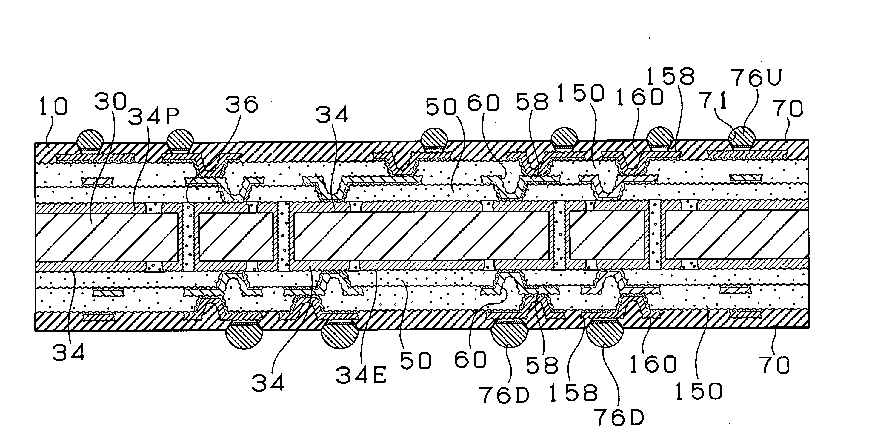
[0018] As a fourth effect, assuming that the side face of the conductive layer of the core substrate is tapered and an angle formed by a straight line connecting the top end and bottom end of the side face of the conductive layer and the horizontal face of the core substrate (hereinafter, called just angle of the side face of the conductive layer depending on a case) is Θ, the Θ satisfies the
relational equation of 2.8<tanΘ<55 and therefore, a
fine structure, prevention of shortage of power and high-speed transmission signal can be achieved at the same time. Because the tan Θ is over 2.8, an interval between the bottom ends of the conductive layer can be secured even if the top ends of the conductive layer are disposed near each other. As a consequence, a high-density printed wiring board having a high insulation reliability is obtained. Further, because a through hole and an inner layer conductor of a core substrate, each having an opposite potential can be disposed near each other,
inductance can be reduced. Thus, a multilayer printed wiring board easy to prevent the shortage of power can be produced. As a method for bringing both to near each other, it is permissible to adopt a through hole having no dummy land, described later. On the other hand, because the tan Θ is less than 55, the side wall of the conductive layer is not at right angle. For the reason, the thickness and
diameter of the conductor of the signal through hole (through hole connected to a signal circuit of the IC electrically) do not need to be reduced to match impedance. As a consequence, conductor resistance of the signal through hole can be reduced, which is advantageous for the transmission of high speed signals. Further, if the side face of the conductive layer is tapered, the shortage of power and deterioration of a signal can be prevented at the same time. Because damping of the signal can be reduced in the signal through hole passing through the multilayer core as it is tapered, deterioration of the signal is unlikely to occur. Further, because an angle of the side face of the conductive layer is over a predetermined angle, conductor resistance can be reduced, thereby suppressing the shortage of power. In case of the multilayer core, when it is assumed that the angle of the side face of the conductive layer on the front and rear surfaces is Θ1 and the angle of the side face of the conductive layer in the inner layer is Θ2, a relation of Θ1>Θ2 is preferred. The reason is that
impedance matching is facilitated on a signal line of built-up
layers because the built-up layer is formed of interlayer
insulation layer and conductive layer on the core substrate. The reason is that when a signal line of the built-up layer is formed on a taper whose Θ1 is small, an area in which the thickness of the interlayer
insulation layer below the signal line differs increases. Further, because the through hole
pitch cannot be decreased,
inductance cannot be reduced.
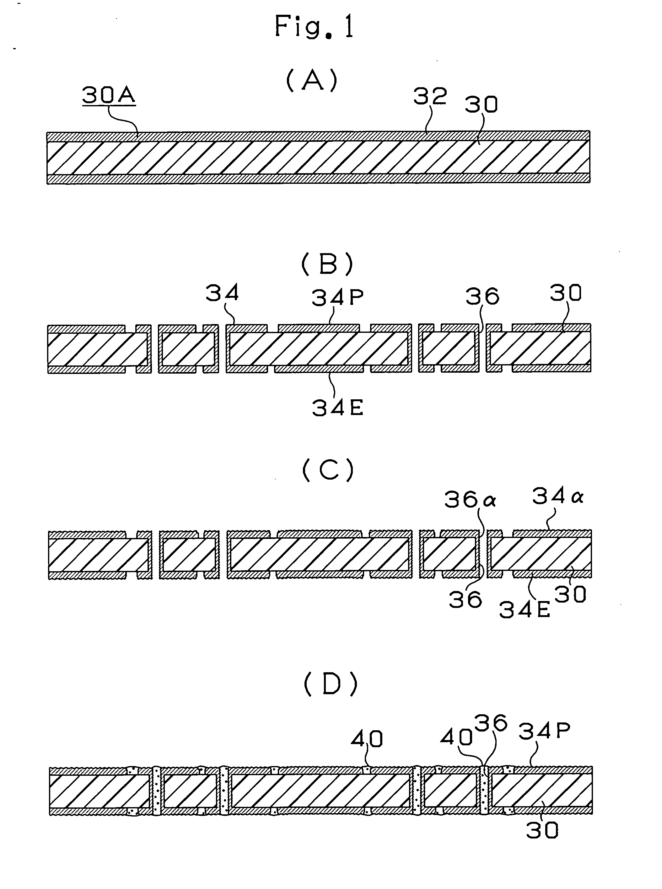
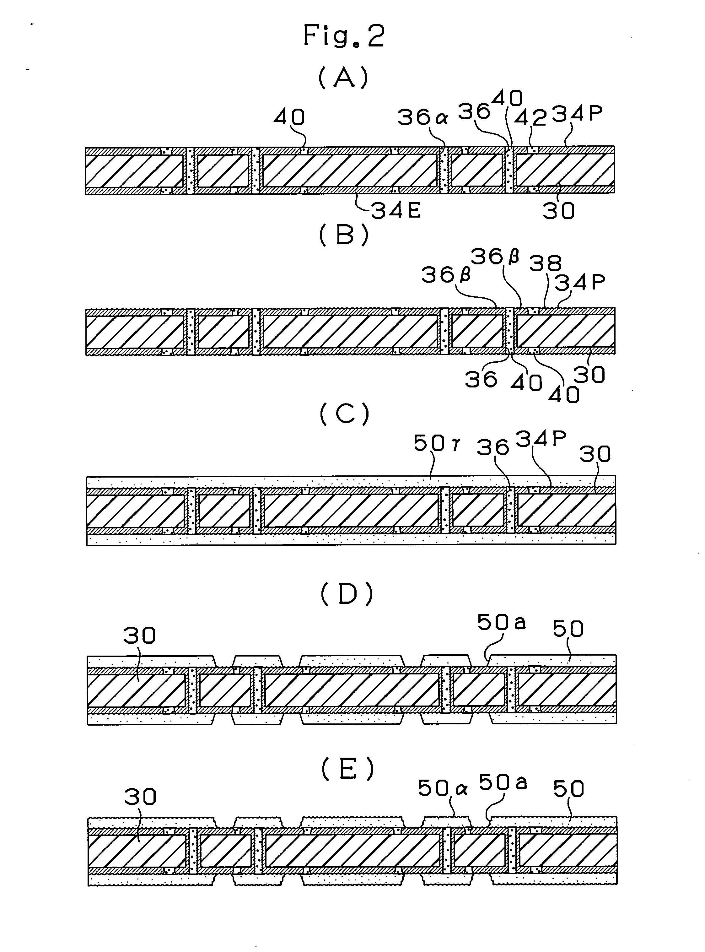
[0019] As a result of accumulated researches for achieving the above-mentioned objects, the inventor and other people have reached the first invention having a following content as its configuration. That is,
[0020] according to a first invention, there is provided a multilayer printed wiring board in which interlayer insulation layer and conductive layer are formed on a core substrate so as to achieve electric connection through via holes, at least one of sums of thicknesses of conductive
layers for power source or for grounding of a core substrate is larger than the thicknesses of the conductive layers on interlayer insulation layer.

