Tmos-infrared uncooled sensor and focal plane array

Active Publication Date: 2006-11-02
TECHNION RES & DEV FOUND LTD
View PDF1 Cites 32 Cited by
  • Summary
  • Abstract
  • Description
  • Claims
  • Application Information

AI Technical Summary

Benefits of technology

[0014] Accordingly, it is a principal object of the present invention to provide an array of uncooled infrared transis

Problems solved by technology

Sensors based on photon counting detectors are very sensitive, but suffer from several drawbacks.
The major disadvantage is that they require significant cooling for their operation, typically down to cryogenic temperatures of about 77° K. As a result, the package of the sensor has to be evacuated to very a high vacuum, and additional cooling means need to be employed.
These demands, of course, increase the cost of the system, and its size and complexity.
The use of exotic semiconductors for the detectors themselves, and the need to use two chips; and bonding them togethe

Method used


Image

  • Tmos-infrared uncooled sensor and focal plane array
  • Tmos-infrared uncooled sensor and focal plane array
  • Tmos-infrared uncooled sensor and focal plane array

Examples


Embodiment Construction

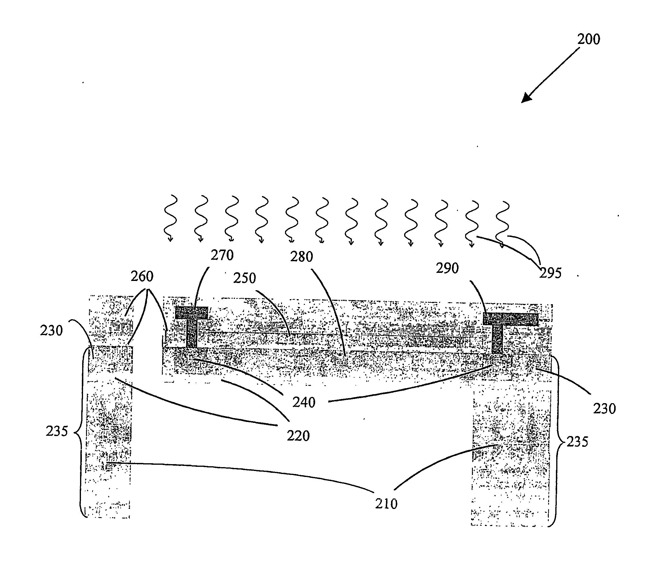
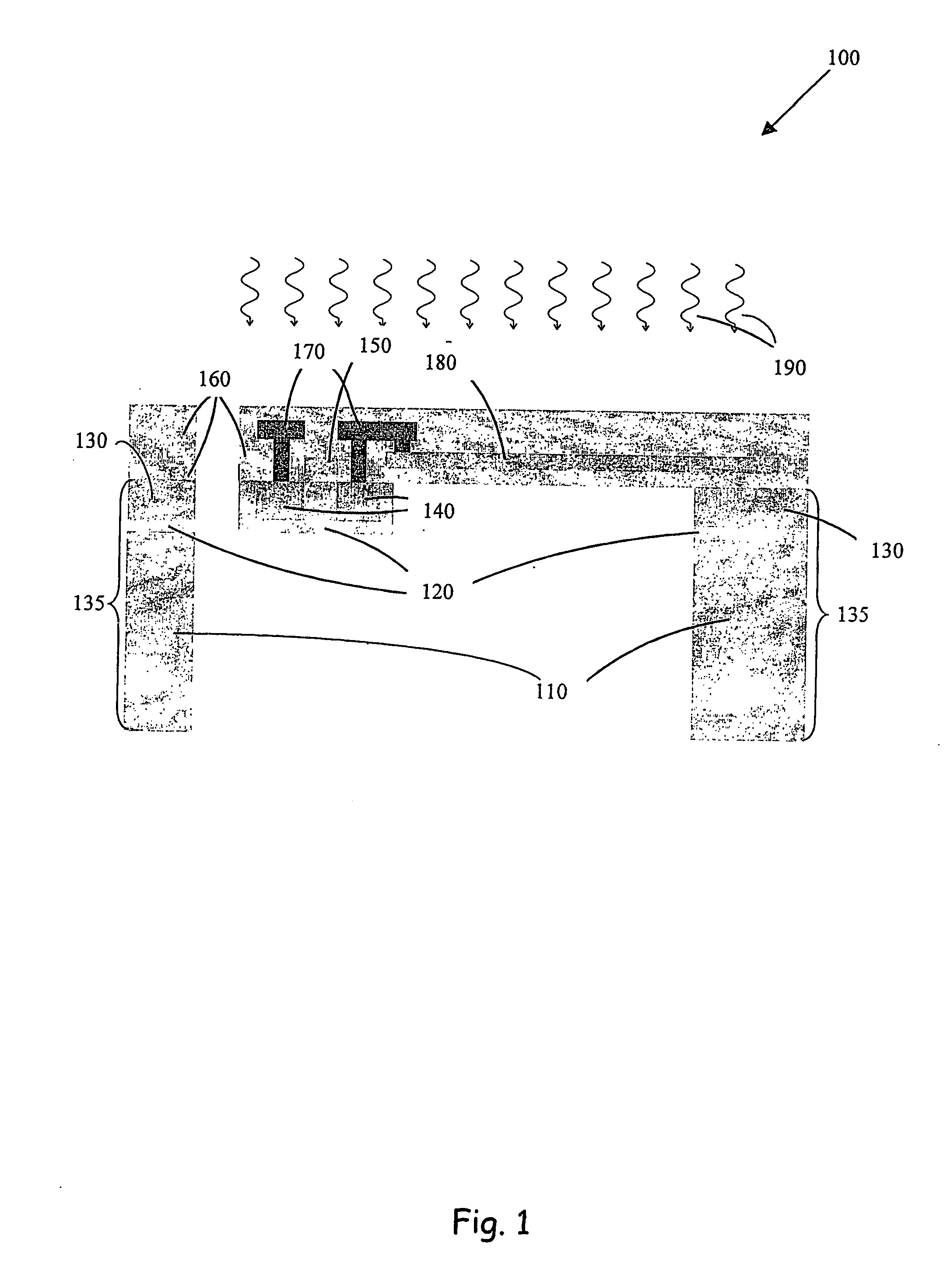
[0027] The invention will now be described in connection with certain preferred embodiments with reference to the following illustrative figures so that it may be more fully understood. References to like numbers indicate like components in all of the figures.

[0028] The infrared uncooled sensor and focal plane array is explained, with reference to FIG. 1, illustrating a cross section of a typical sensor pixel 100 of a Thermally isolated Metal Oxide Semiconductor (TMOS) transistor on a silicon-on-insulator (SOI) substrate that responds with current, threshold voltage and gain changes to infrared radiation, constructed in accordance with the principles of the present invention.

[0029] The sensor structure is based on a single crystal silicon bulk 110, preferably micromachined using an anisotropic deep silicon reactive ion etching (DRIE). A buried thin silicon dioxide layer 120 serves as an etch stop layer for the bulk micromachining process and separates the bulk silicon from the thi...


PUM


Abstract

An array of uncooled infrared sensors based on a micro-machined temperature sensitive MOS transistor. The sensor array is fabricated using a commercial CMOS process on SOI wafers, followed by backside silicon dry etching for each sensor pixel. Active sensor pixels may include either, an integrator and buffer, or simply the sensing transistor, serving also as the selection device. The transistor bias controls the selected device and the sensitivity of the sensor. PMOS transistors and switched operation are used for noise minimization.

Description

FIELD OF INVENTION [0001] The present invention relates to micromachining and micro-sensor arrays. More particularly, the present invention relates to an array of uncooled infrared transistor-based thermal sensors for use in micromachining and microsensors for Thermally isolated Metal Oxide Semiconductors (TMOS). BACKGROUND OF THE INVENTION [0002] Thermal sensors are sensors that detect temperature changes at distant targets through the changes in radiation they emit. Since most objects can be treated as physical “black bodies,” the amount and the spectrum of radiation they emit strongly depend upon their temperature. The amount of radiation increases with temperature, and the peak wavelength of that emission decreases with temperature, such that objects at room temperature of 300° K. have a peak wavelength at the far infrared range of about 10 μm, while the Sun, with a surface temperature of 6000° K., has a peak wavelength at the visible green (0.5 μm). Therefore, sensors that are ...

Claims


Application Information

Patent Timeline
IPC IPC(8): H01L27/12H01L27/01H01L31/0392B81BG02B5/08H02N1/00
CPCB81B3/0062B81B2201/042B81B2203/058B81C2201/019H02N1/006G01J2005/0077G02B26/0841H01L27/1203H01L27/14669G01J5/20
Inventor SOCHER, ERANBOCHOBZA-DEGANI, OFLRNEMIROVSKY, YAEL
Owner TECHNION RES & DEV FOUND LTD
Why Eureka
Try Eureka