Ultrathin porous nanoscale membranes, methods of making, and uses thereof

a nanoscale membrane and ultra-porous technology, applied in the field of ultra-porous nanoscale membranes, can solve the problems of inability to achieve small pores that eventually clog with small molecules, and inability to use in rapid separation procedures. large-scale production of this type of membrane is impractical, and the process could be very easily automated, cost-effective, and not time-consuming

Active Publication Date: 2006-12-14
UNIVERSITY OF ROCHESTER
View PDF81 Cites 120 Cited by
  • Summary
  • Abstract
  • Description
  • Claims
  • Application Information

AI Technical Summary

Benefits of technology

[0019] The method of producing ultrathin nanoscale membranes of the present invention achieves a reproducible and cost-effective approach for the production of membranes that will be commercially useful in filtration, electron microscopy, nanobioreactor applications, and fuel cells. In particular, because the semiconductor materials are rendered porous in a step that allows all pores simultaneously to form during the annealing process, the pore density and size can be controlled by manipulating the annealing conditions and the thickness of the deposited semiconductor material. Moreover, because of the use of sacrificial layers on one or both sides of the semiconductor film that is to form the final membrane, it is possible to prepare membranes with substantially smooth surfaces. This type of local smoothness is a useful feature for filters to be used...

Problems solved by technology

Filters manufactured in this manner naturally contain a wide distribution of pore sizes and the smallest pores will eventually clog with small molecules of the filtrate.
Thus, while the use of channel-type nanomembranes for steady separations is possible, their use in rapid separation procedures seems unlikely.
Large scale production of this type of membrane is impracti...

Method used


Image

  • Ultrathin porous nanoscale membranes, methods of making, and uses thereof
  • Ultrathin porous nanoscale membranes, methods of making, and uses thereof
  • Ultrathin porous nanoscale membranes, methods of making, and uses thereof

Examples


example 1

Formation of Nanocrystalline Silicon Membranes

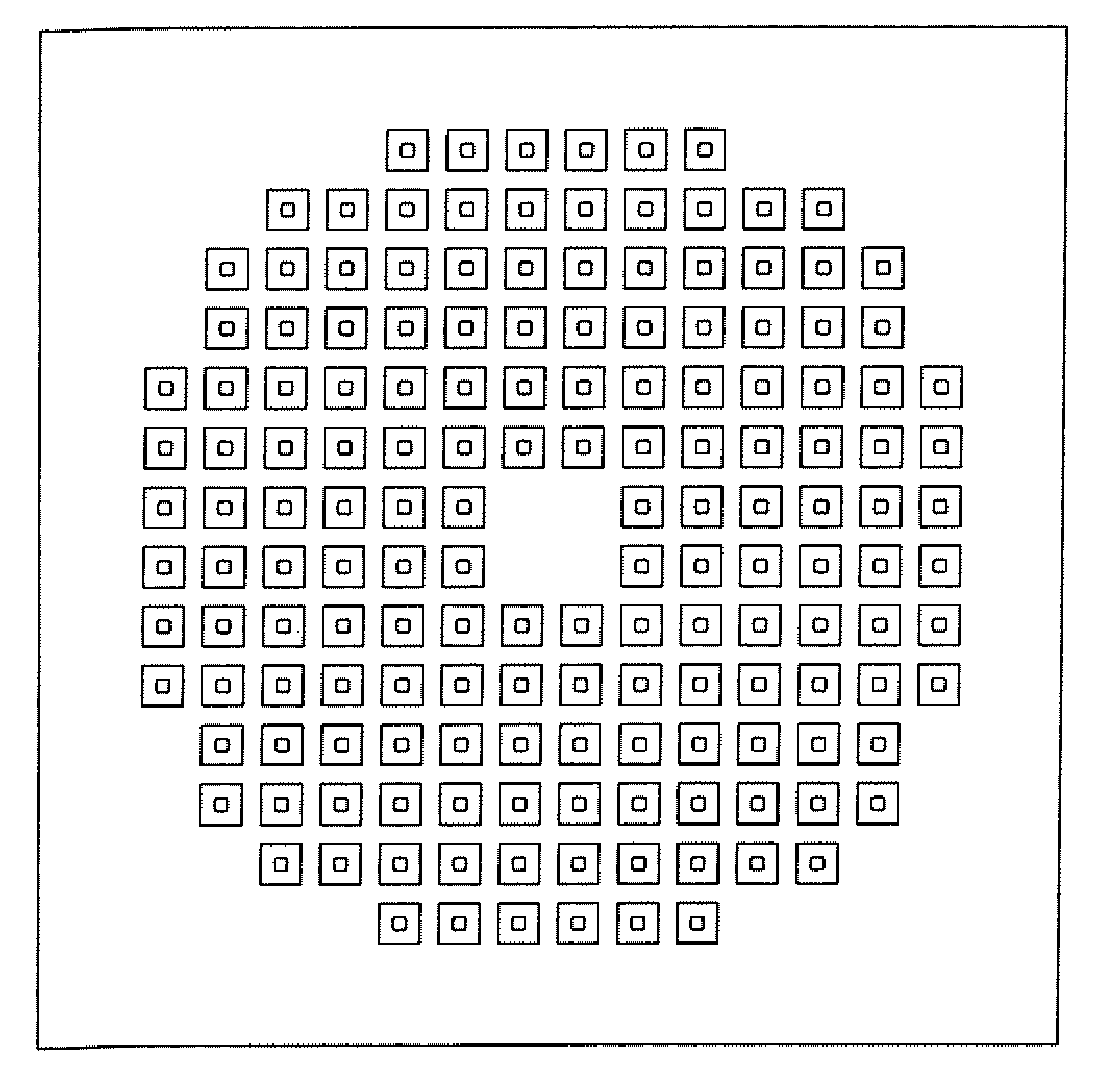
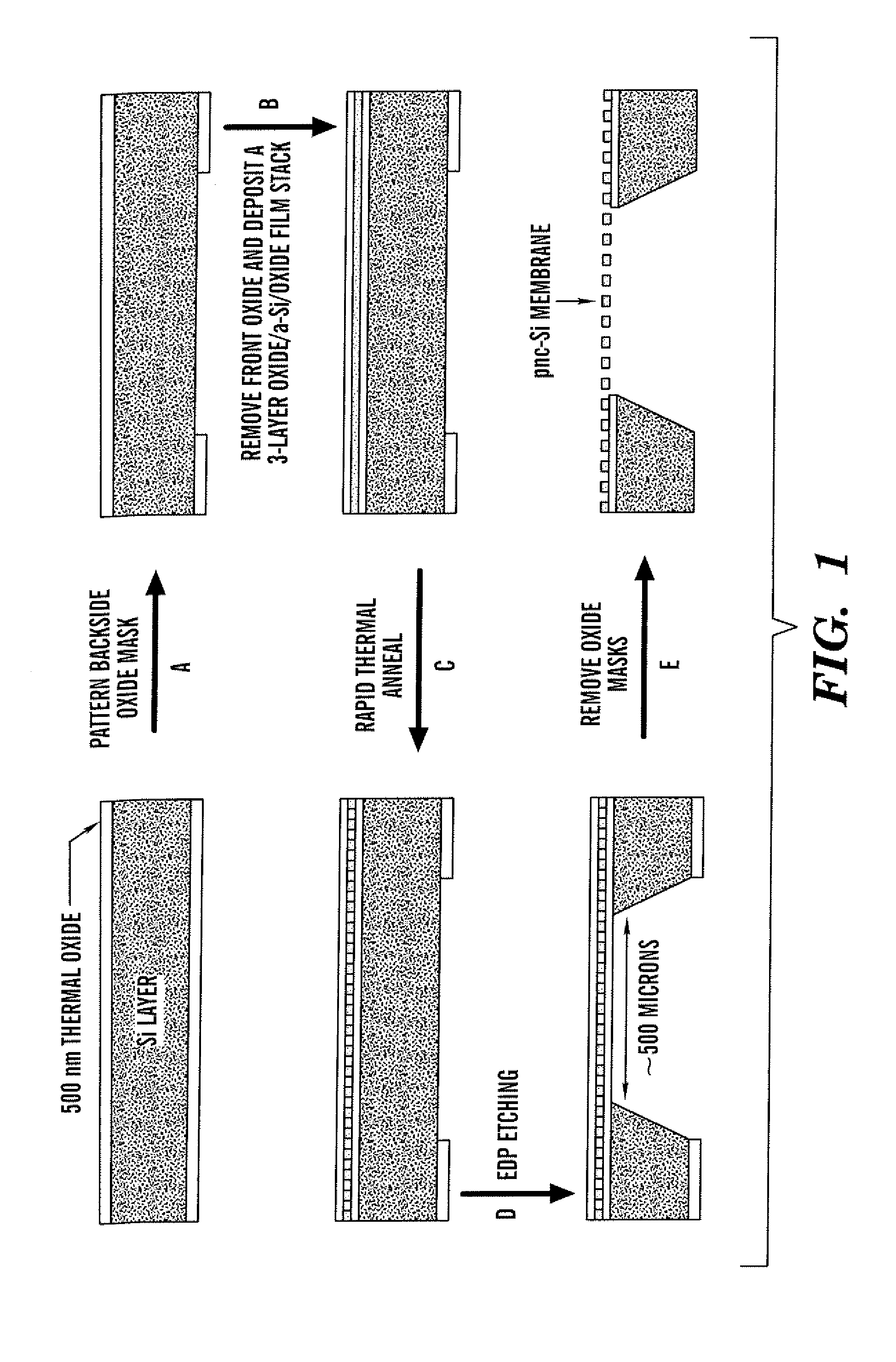
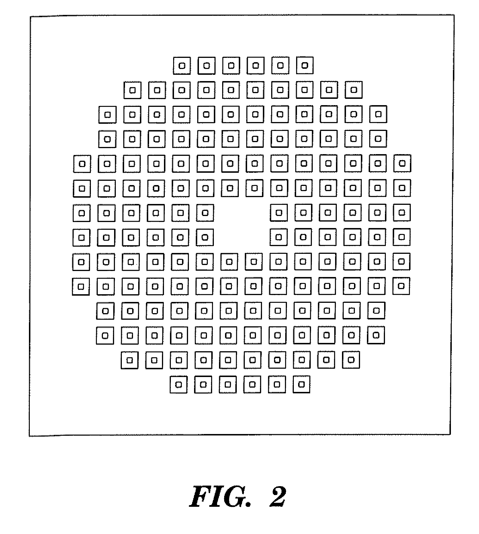
[0112] Pnc-Si membranes were fabricated by the procedure outlined in FIG. 1. A 500 nm thick layer of SiO2 on both sides of a silicon wafer was first grown by placing it in a semiconductor tube furnace at 1000° C. for 2 hours in an ambient of oxygen and steam. On the backside of the wafer, the SiO2 was patterned using standard photolithography techniques to form an etch mask for the membrane formation process. The etch mask for each membrane included a square-shaped opening centrally positioned within a square border (up to 120 masks have been formed on a single silicon wafer). The front oxide layer was then removed by exposing the surface to 4:1 BOE, for 10 minutes, in an etching cell similar to that used for EDP etching, and a high quality three layer film stack (20 nm-SiO2 / 15 nm-amorphous silicon / 20 nm-SiO2) was RF magnetron sputter deposited on the front surface. The a-Si layer was sputtered at a chamber pressure of 15 mTorr in Ar wi...

example 2

Formation of Additional Nanocrystalline Silicon Membrane

[0117] The procedure described in Example 1 was used to form a 7 nm a-Si layer sandwiched between two 20 nm layers of SiO2 using sputter deposition; the silicon was then annealed at 950° C. for 30 sec to form a nc-Si layer. After release, a wrinkled membrane similar to other oxide membranes was formed (FIG. 10A). However, after the removal of the sacrificial SiO2, with a 25 second dip in buffered oxide etch (BOE), an extremely flat 7 nm ne-Si membrane was produced (see FIGS. 10B-C). This dramatic shift from compressive to tensile stress was unexpected, yet is indicative of the volume contraction that occurs when a-Si is crystallized (Miura et al., Appl. Phys. Lett. 60:2746 (1992), Zacharias et al., Journal of Non-Crystalline Solids 227-230:1132 (1998), which are hereby incorporated by reference in their entirety). Since the oxide remains compressively stressed after annealing and is much thicker than the a-Si, the overall film...

example 3

Physical Properties of Porous Nanocrystalline Silicon Membranes

[0122] In addition to TEM, several other characterization techniques have been used to confirm the properties of the pnc-Si membranes according to the present invention. FIG. 9A shows refractive index dispersion data obtained using spectroscopic ellipsometry for a 15 nm thick silicon film after deposition (a-Si) and after crystallization (pnc-Si) (Tompkins et al., “Spectroscopic Ellipsometry and Reflectometry—A User's Guide,”Wiley &Sons, Inc., New York, (1999), which is hereby incorporated by reference in its entirety). The sputtered a-Si has high optical density, comparable to microelectronic quality a-Si deposited with chemical vapor deposition (CVD), and exhibits a clear shift in optical properties after crystallization, with characteristic resonance peaks similar to crystalline silicon (Palik, E. D. “Handbook of Optical Constants of Solids,” (Academic Press, Orlando) pp. 547-569 (1985), which is hereby incorporated ...


PUM

PropertyMeasurementUnit
Pore sizeaaaaaaaaaa
Thicknessaaaaaaaaaa
Thicknessaaaaaaaaaa

Abstract

A process for forming a porous nanoscale membrane is described. The process involves applying a nanoscale film to one side of a substrate, where the nanoscale film includes a semiconductor material; masking an opposite side of the substrate; etching the substrate, beginning from the masked opposite side of the substrate and continuing until a passage is formed through the substrate, thereby exposing the film on both sides thereof to form a membrane; and then simultaneously forming a plurality of randomly spaced pores in the membrane. The resulting porous nanoscale membranes, characterized by substantially smooth surfaces, high pore densities, and high aspect ratio dimensions, can be used in filtration devices, microfluidic devices, fuel cell membranes, and as electron microscopy substrates.

Description

[0001] This application claims the benefit of U.S. Provisional Patent Application Ser. Nos. 60 / 675,963 and 60 / 782,001 filed Apr. 29, 2005, and Mar. 14, 2006, respectively, which are hereby incorporated by reference in their entirety.FIELD OF THE INVENTION [0002] The present invention relates to porous nanoscale membranes, particularly ultrathin porous nanoscale membranes, methods of making the membranes, and uses thereof. BACKGROUND OF THE INVENTION [0003] The separation of molecules in biological fluids is a basic procedure important in clinical diagnosis and disease treatment, and the most elemental device for solute separation is a porous membrane filter. Thus, a revolutionary advance in filter technology has the potential to impact many areas of human health. Typical filter materials are made as woven matrices of plastic or cellulose polymers. Filters manufactured in this manner naturally contain a wide distribution of pore sizes and the smallest pores will eventually clog with ...

Claims


Application Information

Patent Timeline
IPC IPC(8): B01D61/00
CPCB01D61/18B01D2325/26B01D67/0062B01D67/0072B01D71/02B01L3/50255B01L2300/0819B01L2400/0472B01L2400/0627H01J2237/20H01M4/94H01M8/1037H01M8/1076H01M2250/00H01M2300/0094Y02E60/521B01D57/02B01D2325/08B01D2325/14B01D61/28Y02P70/50Y02E60/50B01D71/0213
Inventor STRIEMER, CHRISTOPHER C.FAUCHET, PHILIPPE M.GABORSKI, THOMAS R.MCGRATH, JAMES L.
Owner UNIVERSITY OF ROCHESTER
Why Eureka
Try Eureka