Abrasive compounds for semiconductor planarization

Inactive Publication Date: 2006-12-21
HITACHI CHEM CO LTD
View PDF6 Cites 10 Cited by
  • Summary
  • Abstract
  • Description
  • Claims
  • Application Information

AI Technical Summary

Benefits of technology

[0016] A surface of a semiconductor can be polished at a high speed in a wiring formation process by the

Problems solved by technology

However, since the polishing speed of the silica polishing slurry is slow, attentions have been recently focused on a cerium oxide polishing slurry containing cerium oxide having a fast polishing speed (for example, see Japanese Patent Application Laid-Open Nos. 2000-26840 and 2-371267).
However, the cerium oxide polishing slurry has a problem of generating more scratches as compared with the silica polishing slurry.
Though it has been presumed that the scratches generated in the polish process relate to the particle diameter of the polishing slurry, quantitive evaluation results have been seldom obtained.
Though it has been considered that the cerium oxide polishing s

Method used


Image

  • Abrasive compounds for semiconductor planarization

Examples


example 1

[0041] Hereinafter, though the present invention is specifically described with reference to examples, the present invention is not limited thereto.

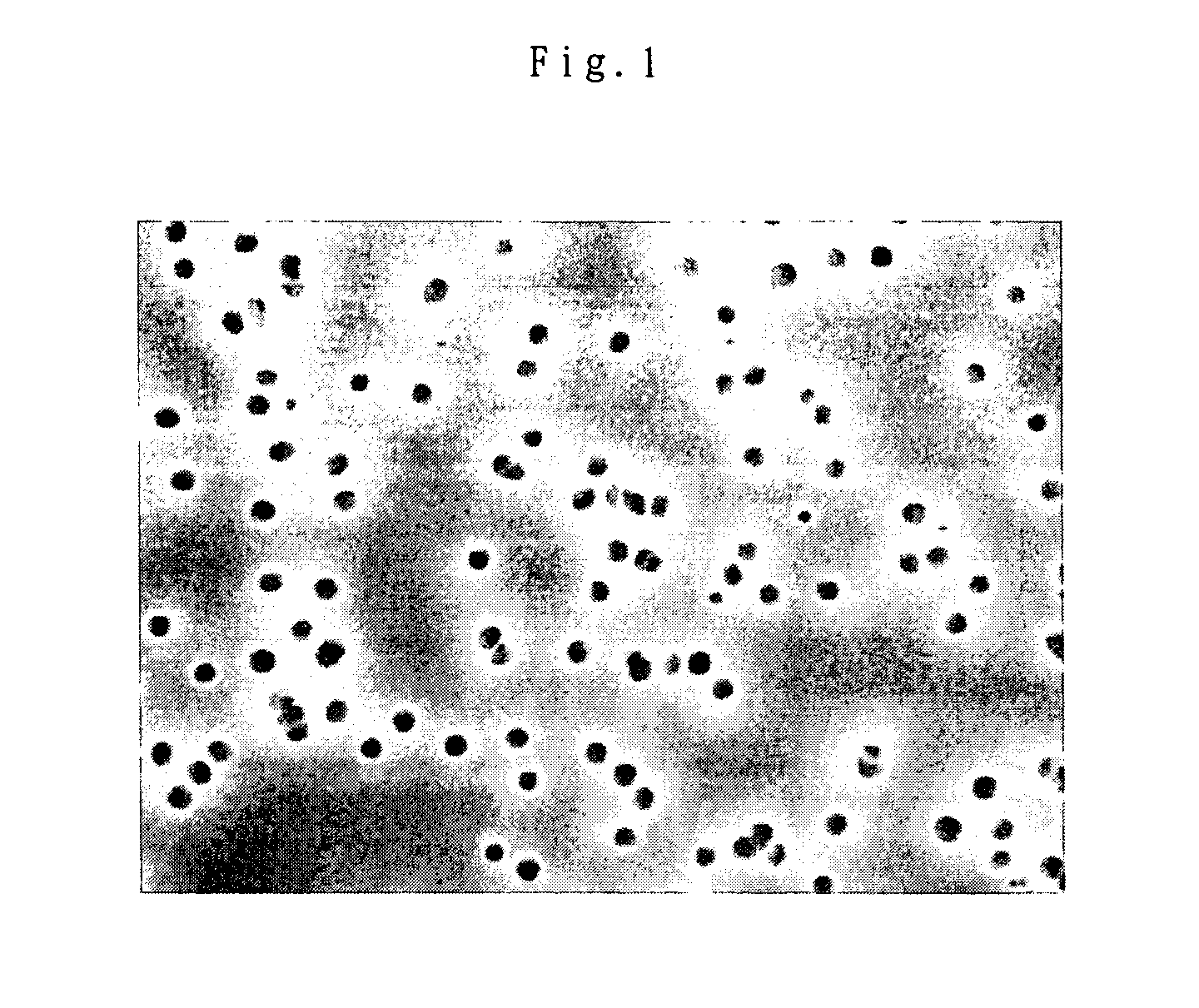
[0042] Commercially available cerium carbonate of about 6 kg was put into an alumina container, and yellowish white powder of about 3 kg was obtained by firing the cerium carbonate at 800° C. in air for 2 hours. The powder was identified by an X-ray diffraction method, and was confirmed to be cerium oxide. The particle diameter of the fired powder was within the range of 30 to 100 μm. Furthermore, the obtained cerium oxide powder of 3 kg was dry grinded by using the jet mill to obtain the cerium oxide particles.

[0043] Cerium oxide particles of 1000 g produced above, an aqueous solution of ammonium polyacrylate of 80 g (40% by weight), and deionized water of 3920 g were mixed, and an ultrasonic distribution was performed for 10 minutes while the mixture was stirred. The obtained dispersion liquid was left and settled out at room tempera...

example 2

[0052] The cerium oxide particles of 1000 g produced in Example 1, an aqueous solution of ammonium polyacrylate of 80 g (40% by weight), and deionized water of 3920 g were mixed, and an ultrasonic distribution was performed for 10 minutes while the mixture was stirred. The obtained dispersion liquid was left and settled out at room temperature for 100 hours, and a supernatant fluid was obtained. After filtering the supernatant fluid through the filter for mass production having the pore diameter of 0.7 μm, it was filtered through the filter for mass production having the pore diameter of 0.7 μm again, and the solid content concentration was adjusted to 5% by adding deionized water to produce a polishing slurry for semiconductor planarization.

[0053] The particle diameter of the obtained polishing slurry for semiconductor planarization was measured in the same manner as Example 1. As a result, the median (D50) of the secondary particle diameters was 160 nm, and the D99 was 0.5 μm. Th...


PUM


Abstract

A polishing slurry for semiconductor planarization containing cerium oxide particles and water, wherein the content of the cerium oxide particles having a diameter of 3 μm or more is 500 ppm or less (weight ratio) in a solid, preferably 100 ppm or less and it is more preferable that D99 (99% by volume of the whole particles in polishing slurry) of the cerium oxide particles is 1 μm or less. The polishing slurry can reduce the generation of scratches, and can polish a surface of the semiconductor substrate in the wiring formation process of semiconductor device precisely at a high speed.

Description

TECHNICAL FIELD [0001] The present invention relates to a polishing slurry, and particularly relates to polishing slurries for semiconductor planarization. BACKGROUND ART [0002] A precise polish process for polishing the surface of a material is required in, for example, optical disk substrates, a magnetic disks, glass substrates for flat panel displays, clock boards, camera lenses, glass material used for various lenses and crystal material for filters or the like for optical components, substrates of a silicon wafer or the like for semiconductors, and insulated films, metal layers and barrier layers or the like formed in each process for manufacturing semiconductor devices. The surfaces of these materials require high accuracy polishing. Therefore, for example, polishing agents have been generally used, using silica, zirconium oxide and alumina or the like alone or in combination of two or more kinds as polish particles. Referring to a form of the polishing agent, for example, a s...

Claims


Application Information

Patent Timeline
IPC IPC(8): B24D3/02B24B37/00C09G1/02C09K3/14H01L21/304
CPCC09G1/02C09K3/1463C09K3/1409H01L21/304
Inventor CHINONE, KANSHI
Owner HITACHI CHEM CO LTD
Why Eureka
Try Eureka