
Field emission display having carbon nanotube emitter and method of manufacturing the same

a carbon nanotube and emitter technology, applied in the manufacture of electric discharge tubes/lamps, discharge tubes luminescnet screens, electrode systems, etc., can solve the problems of short life of silicon tips and molybdenum tips, low electron emission efficiency, low stability, etc., to achieve excellent step coverage, reduce stress, and the effect of sufficient thickness

Inactive Publication Date: 2006-12-28
SAMSUNG SDI CO LTD
View PDF4 Cites 5 Cited by
  • Summary
  • Abstract
  • Description
  • Claims
  • Application Information

AI Technical Summary

Benefits of technology

[0011] It is also an object of the present invention to provide a design for an FED that does not result in delamination of layers or cracks in layers, without causing other adverse effects.
[0027] The CNT FED according to the present invention includes a focus gate insulating film by which an excellent step coverage is obtained between the focus gate electrode and the gate electrode and which has an enough thickness to minimize stresses between the focus gate electrode and the gate electrode. Therefore, defects such as cracks are not generated in the focus gate insulating film, thus reducing leakage current between the focus gate electrode and the gate electrode. Since the focus gate insulating film has a sufficiently large thickness, the focus gate electrode and the gate electrode are separated away from each other by a distance corresponding to the large thickness. Therefore, an insulation breakage between the two electrodes by impurities adhering to the focus gate insulating film can be avoided. Also, the manufacturing process can be simplified because the photosensitive film is patterned by self-alignment instead of using an additional mask, thus reducing manufacturing costs.

Problems solved by technology

However, both silicon tips and molybdenum tips have short lifetimes, low stability, and low electron emission efficiency.
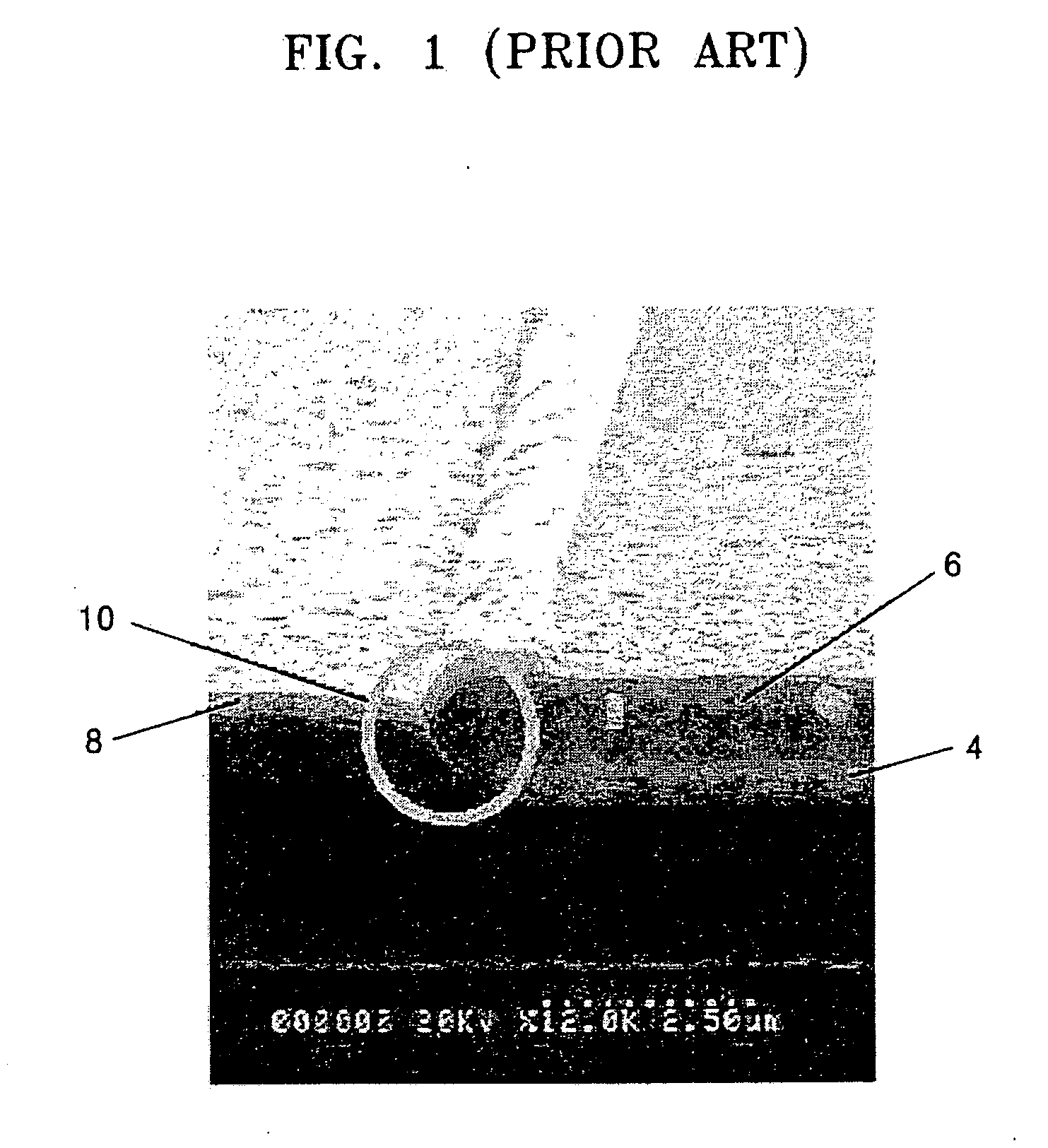
This poor step coverage can result in electrical defects such as the crack 10 illustrated in FIG. 1 that causes insulating breakage at the step portion.
Such defect could generate a leakage current between the two electrodes, thus generating joule heat at the step portion.
However, it is not easy to obtain a desirable thickness because delamination occurs when the thickness of the silicon oxide film is increased to over 2 μm.
In the former case, a possibility of crack formation between a focus gate electrode and a gate electrode used to extract electrons is low, but an outgassing process for venting gas generated by polyimide is required because the focus gate electrode is formed on polyimide.
However, processing and bonding the metal mesh are difficult, and in particular, an electron beam may be shifted due to misalignment of the metal mesh.

Method used


Image

  • Field emission display having carbon nanotube emitter and method of manufacturing the same
  • Field emission display having carbon nanotube emitter and method of manufacturing the same
  • Field emission display having carbon nanotube emitter and method of manufacturing the same

Examples


Embodiment Construction

[0045] The present invention will now be described more fully with reference to the accompanying drawings in which exemplary embodiments of the invention are shown. In the drawings, the thicknesses of layers and regions are exaggerated for clarity. A carbon nanotube field emission display (CNT FED) according to the present invention will be described.

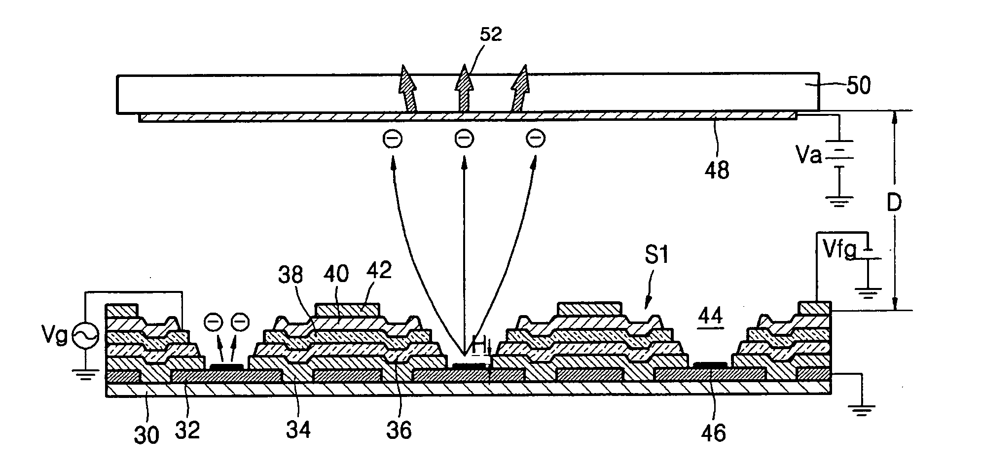
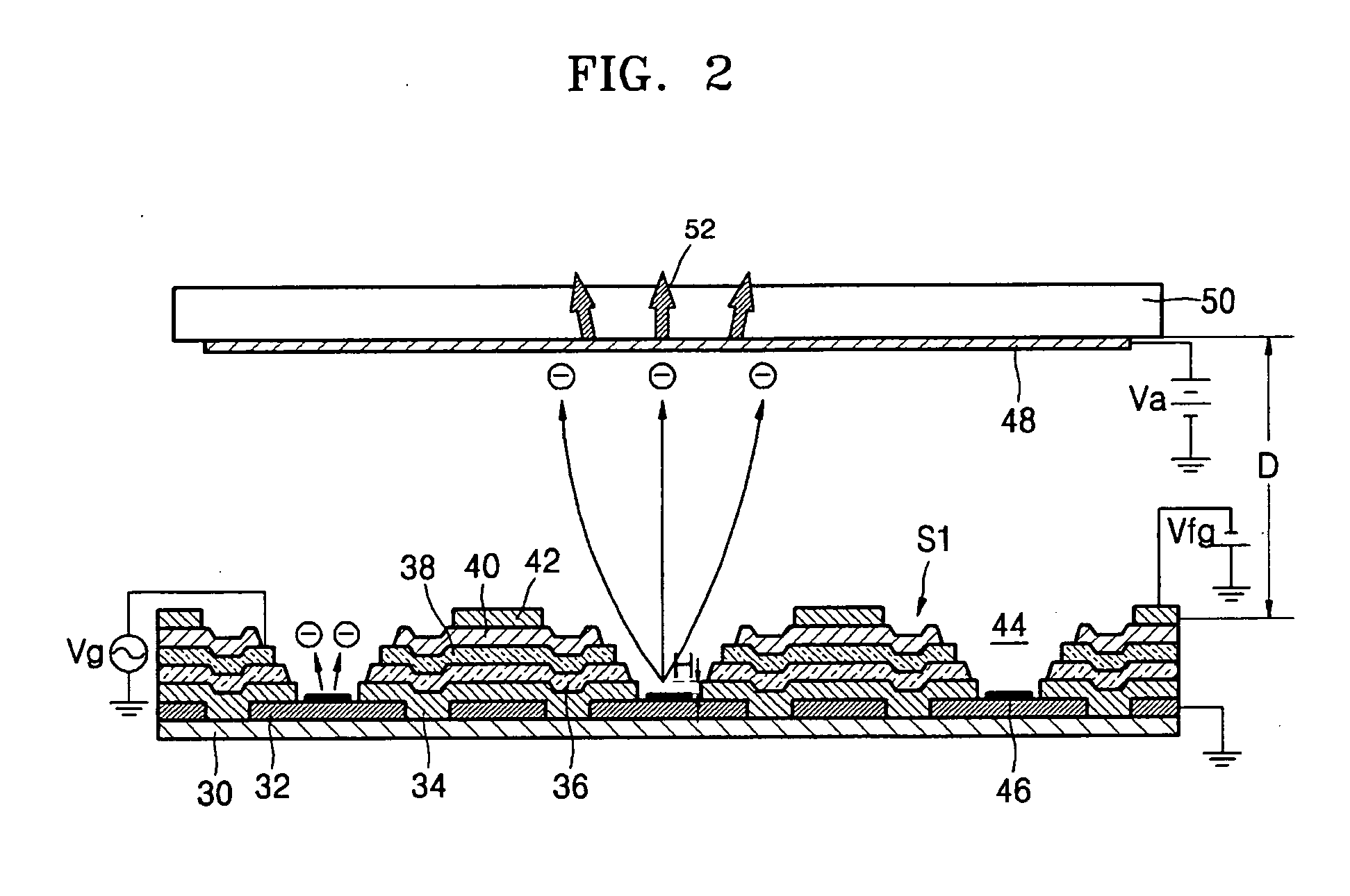
[0046] Turning to FIG. 2, FIG. 2 is a cross-sectional view of an FED that includes a CNT emitter according to an exemplary embodiment of the present invention. Referring to FIG. 2, transparent electrodes 32 are formed on a glass substrate 30. The transparent electrodes 32 may be indium tin oxide (ITO) electrodes and may serve as emitter electrodes. Gate stacks S1 that cover a portion of the transparent electrodes 32 are formed on the glass substrate 30. There are contact holes 44 that expose portions of the transparent electrodes 32 between the gate stacks S1. CNT emitters 46 that emit electrons are formed on a portion of the transpare...


PUM


Abstract

A field emission display (FED) using carbon nanotube emitters and a method of manufacturing the same. A gate stack that surrounds the CNT emitter includes a mask layer that covers an emitter electrode adjacent to the CNT emitter, and a gate insulating film, a gate electrode, a focus gate insulating film (SiOX, X<2), and a focus gate electrode formed on the mask layer. The height of the mask layer is greater than that of the CNT emitter. The focus gate insulating film has a thickness 2 μm or more, and preferably 3˜15 μm. In a process of forming the focus gate insulating film and / or the gate insulating film, a flow rate of silane is maintained at 50˜700 sccm and a flow rate of nitric acid (N2O) is maintained at 700˜4,500 sccm.

Description

CLAIM OF PRIORITY [0001] This application makes reference to, incorporates the same herein, and claims all benefits accruing under 35 U.S.C. §119 from an application for FIELD EMISSION DISPLAY HAVING CARBON NANOTUBE EMITTER AND METHOD OF MANUFACTURING THE SAME earlier filed in the Korean Intellectual Property Office on 26 Jul. 2004 and there duly assigned Serial No. 10-2004-0058348. BACKGROUND OF THE INVENTION [0002] 1. Field of the Invention [0003] A flat display panel and a method of manufacturing the same, and more particularly, to a field emission display having a carbon nanotube emitter and a method of manufacturing the same. [0004] 2. Description of the Related Art [0005] It is readily predicted that cathode ray tubes will be superceded by flat display panels such as liquid displays, light emitting diodes, plasma display panels, and field emission displays (FED). Among these, the FED, which has advantages of high resolution, high efficiency, and low power consumption, receives...

Claims


Application Information

Patent Timeline
IPC IPC(8): H01J63/04
CPCB82Y10/00H01J9/025H01J2201/30469H01J29/481H01J31/127H01J29/04B82Y40/00H01J1/304
Inventor CHOI, JUN-HEEZOULKARNEEV, ANDREIKANG, HO-SUKSHIN, MOON-JIN
Owner SAMSUNG SDI CO LTD
Learn More