Fabrication of quantum dots embedded in three-dimensional photonic crystal lattice

Inactive Publication Date: 2007-01-04
UNIVERSITY OF DELAWARE
View PDF18 Cites 19 Cited by
  • Summary
  • Abstract
  • Description
  • Claims
  • Application Information

AI Technical Summary

Benefits of technology

[0010] The QD-s produced by the method are electrically connected (e.g., through silicon veins) to a bulk silicon substrate and to the top surface of patterned silicon. In the case of a laser, for example, the top electrode(e.g., metal) is optically isolated from the structure producing light by the intervening photonic crystal allowing for optical isolation of the optical mode from the metal, and thereby minimizing optical losses.
[0011] By having the electrical connections going only through the QD-s without the ability to bypass them, pumping efficiency is improved by using all the cur

Problems solved by technology

Light emission in bulk silicon presents a challenge because Si is an indirect bandgap material, therefore radiative transition requires phonon assistance, and therefore the transition has low probability so that non-radiative processes dominate.
Difficulties with QD-s previously realized include the fact that QD-s were embedded in an SiO2 matrix, which provides poor conductivity for electrical pumping.
Reducing QD separation to improve conductivity (e.g., by tunneling) compromises the dot isolation required for electron/hole quantum confinement, and therefore compromises

Method used


Image

  • Fabrication of quantum dots embedded in three-dimensional photonic crystal lattice
  • Fabrication of quantum dots embedded in three-dimensional photonic crystal lattice
  • Fabrication of quantum dots embedded in three-dimensional photonic crystal lattice

Examples


Embodiment Construction

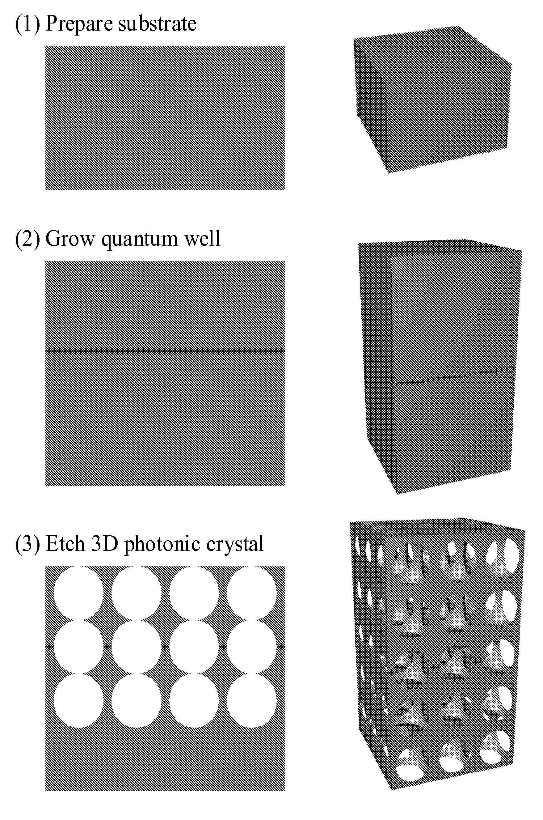
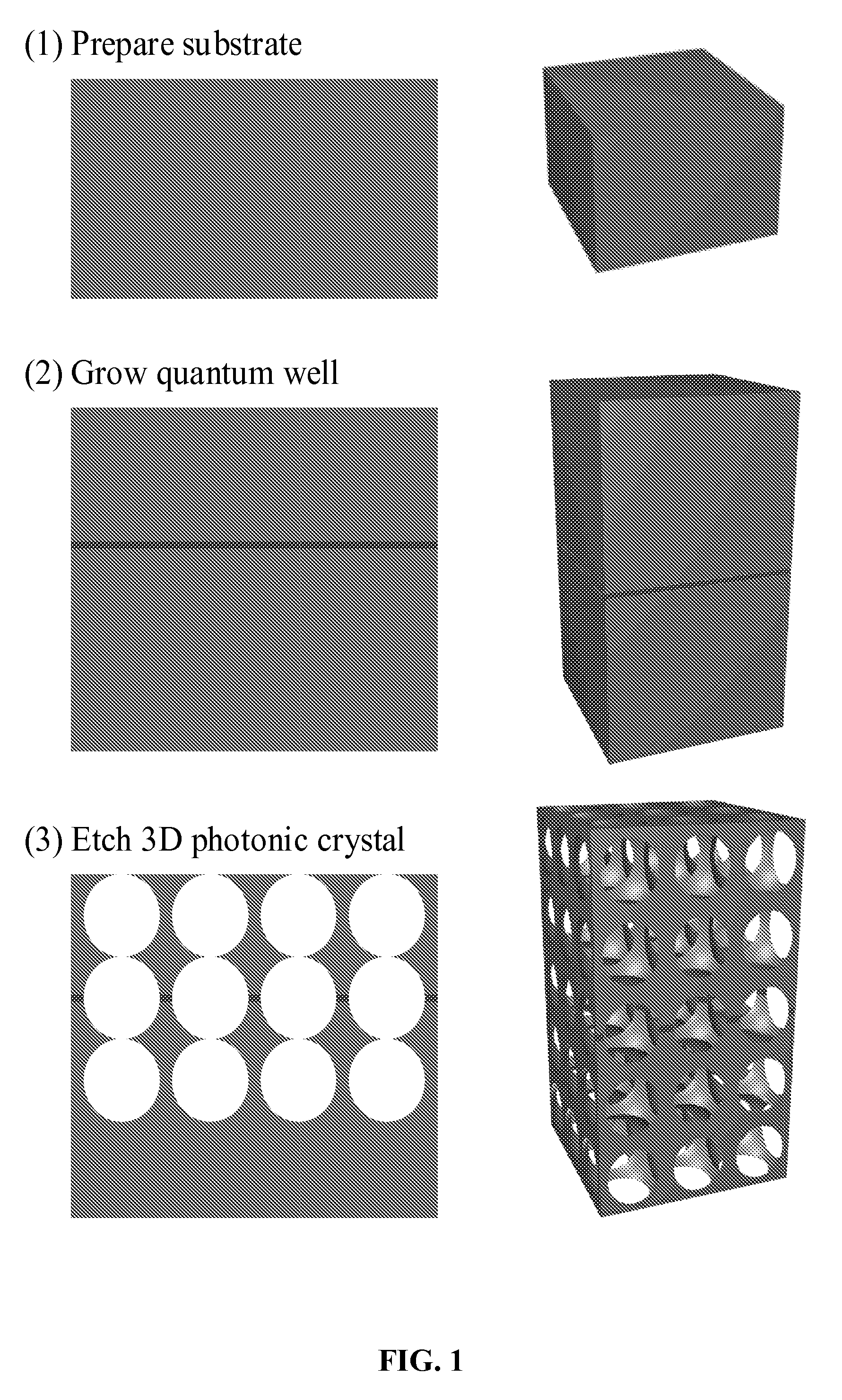
[0021] This disclosure provides a fabrication method that allows deterministic and easy placement of QD-s inside a 3-D photonic crystal lattice to be achieved, and which provides a path for electrical pumping of QD-s. Further, leak current bypassing QD-s is suppressed, and metal electrodes are optically isolated from, but electrically connected with QD-s. In addition, QD-s are passivated as part of the fabrication process, thus improving the stability of the devices. Homogeneous QD size and high density of isolated QD-s are possible.

[0022] The method and structure of this disclosure overcome the difficulties of conventional approaches. Photonic crystal structures provide natural pathways for current, thereby allowing convenient electrical pumping. The conductivity can be selectively enhanced by doping during crystal growth, e.g., during epitaxial growth. All pumping current necessarily passes through quantum dots, resulting in efficient pumping. The pumping electrodes are optically...


PUM


Abstract

In one embodiment, a method of producing an optoelectronic nanostructure includes preparing a substrate; providing a quantum well layer on the substrate; etching a volume of the substrate to produce a photonic crystal. The quantum dots are produced at multiple intersections of the quantum well layer within the photonic crystal. Multiple quantum well layers may also be provided so as to form multiple vertically aligned quantum dots. In another embodiment, an optoelectronic nanostructure includes a photonic crystal having a plurality of voids and interconnecting veins; a plurality of quantum dots arranged between the plurality of voids, wherein an electrical connection is provided to one or more of the plurality of quantum dots through an associated interconnecting vein.

Description

CROSS-REFERENCE TO RELATED APPLICATIONS [0001] This application claims benefit under 35 U.S.C. §119(e) to U.S. Provisional Application 60 / 696,245 filed on Jul. 1, 2005, the entire contents of which are incorporated herein by reference.BACKGROUND [0002] This application is related to processes suitable for producing nanostructures in the form of quantum dots (“QD-s”) in silicon (Si). This disclosure is more particularly related to a new process for fabricating nanostructures in the form of QD-s in epitaxially grown silicon. [0003] Quantum dots form when very thin semiconductor films buckle due to the stress of having lattice structures slightly different in size from those of the material upon which the films are grown. [0004] The small size of QD-s results in new quantum phenomena that yield desirable effects. Material properties change dramatically because quantum effects arise from the confinement of electrons and holes in the material. The small size changes other material proper...

Claims


Application Information

Patent Timeline
IPC IPC(8): H01L31/00
CPCB82Y10/00B82Y20/00G02B6/10Y10S977/814Y10S977/778Y10S977/774G02B6/1225Y10T428/249953Y10T428/249969
Inventor MURAKOWSKI, JANUSZSCHNEIDER, GARRETTPRATHER, DENNIS W.
Owner UNIVERSITY OF DELAWARE
Why Eureka
Try Eureka