Device for improving plasma activity PVD-reactors

a technology of plasma activity and reactor, which is applied in the direction of electrolysis components, vacuum evaporation coatings, coatings, etc., can solve the problems of risky impact damage to substrates, and achieve the effects of improving plasma activity, increasing plasma intensity, and keeping the technology simpl

Inactive Publication Date: 2007-01-25
SANDVIK INTELLECTUAL PROPERTY AB
View PDF16 Cites 33 Cited by
  • Summary
  • Abstract
  • Description
  • Claims
  • Application Information

AI Technical Summary

Benefits of technology

[0011] It is thus an object of the present invention to provide a device and a method for increasing the plasma intensity during sputter-etching of substrates while keeping the technology simple.
[0012] In one aspect of the invention there is provided a device for improving plasma activity in a coating reactor containing substrates to be coated, where a primary plasma is created by a DC or AC voltage applied between the substrates and at least one additional electrode, said device comprising a thermionic emitter, h

Problems solved by technology

The voltage necessary to operate the discharge was

Method used


Image

  • Device for improving plasma activity PVD-reactors
  • Device for improving plasma activity PVD-reactors
  • Device for improving plasma activity PVD-reactors

Examples


example 1

Prior Art

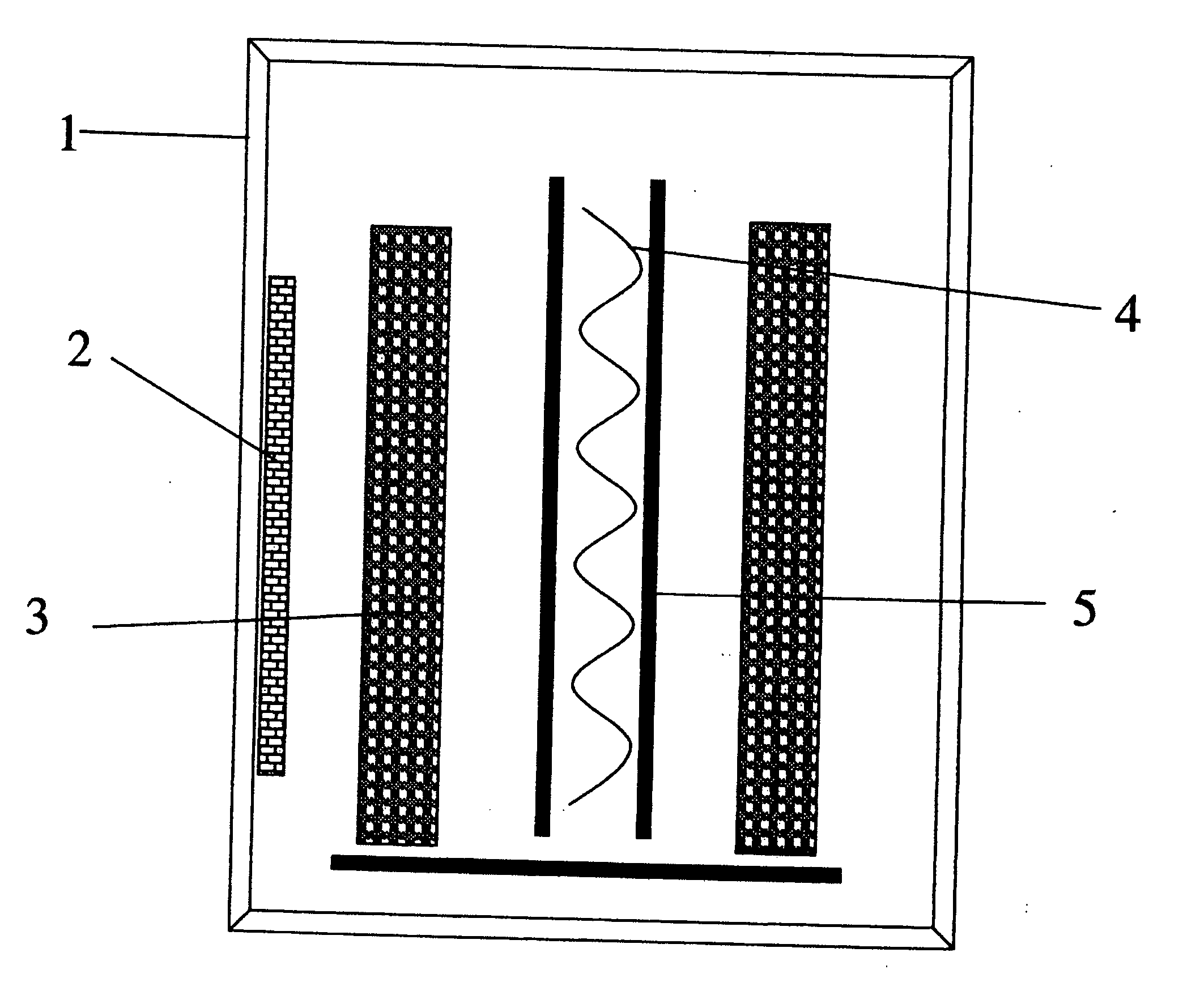
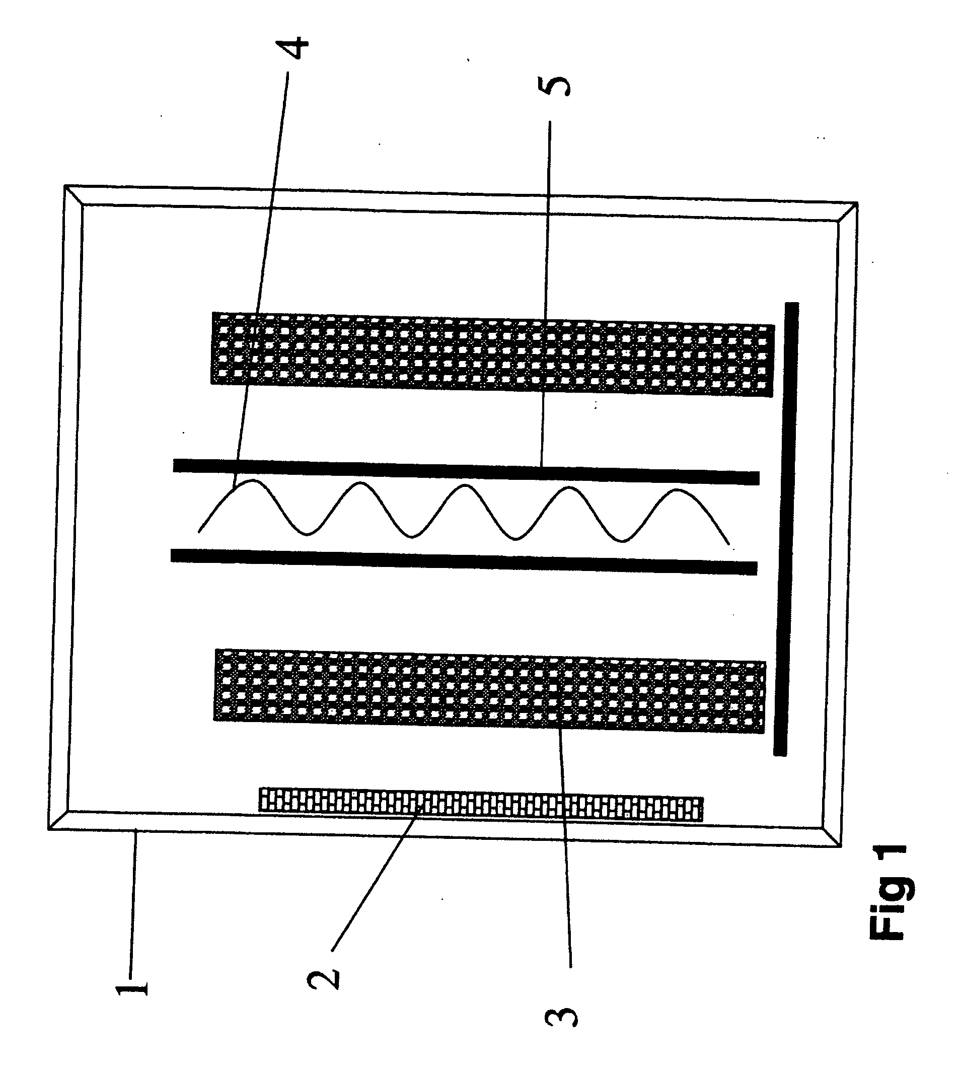
[0028] Sputter etching of cemented carbide cutting inserts was performed according to the system described in WO 97 / 22988. A plasma was ignited at a moderate pressure of 0.8 Pa and a substrate-target voltage of 800 V, which was the minimum voltage to operate the etching. A current flowing through the substrates of 2 A was achieved. This substrate current was limited by the ion density resulting from using a magnetron as counter electrode. The current was, furthermore, related to the impact by charged ions and was thus a measure of the etch. The substrates showed after this sputter-etching procedure signs of redeposition on shadowed surfaces. The voltage necessary to operate the discharge was high enough to risk impact damage to the substrates.

example 2

Invention

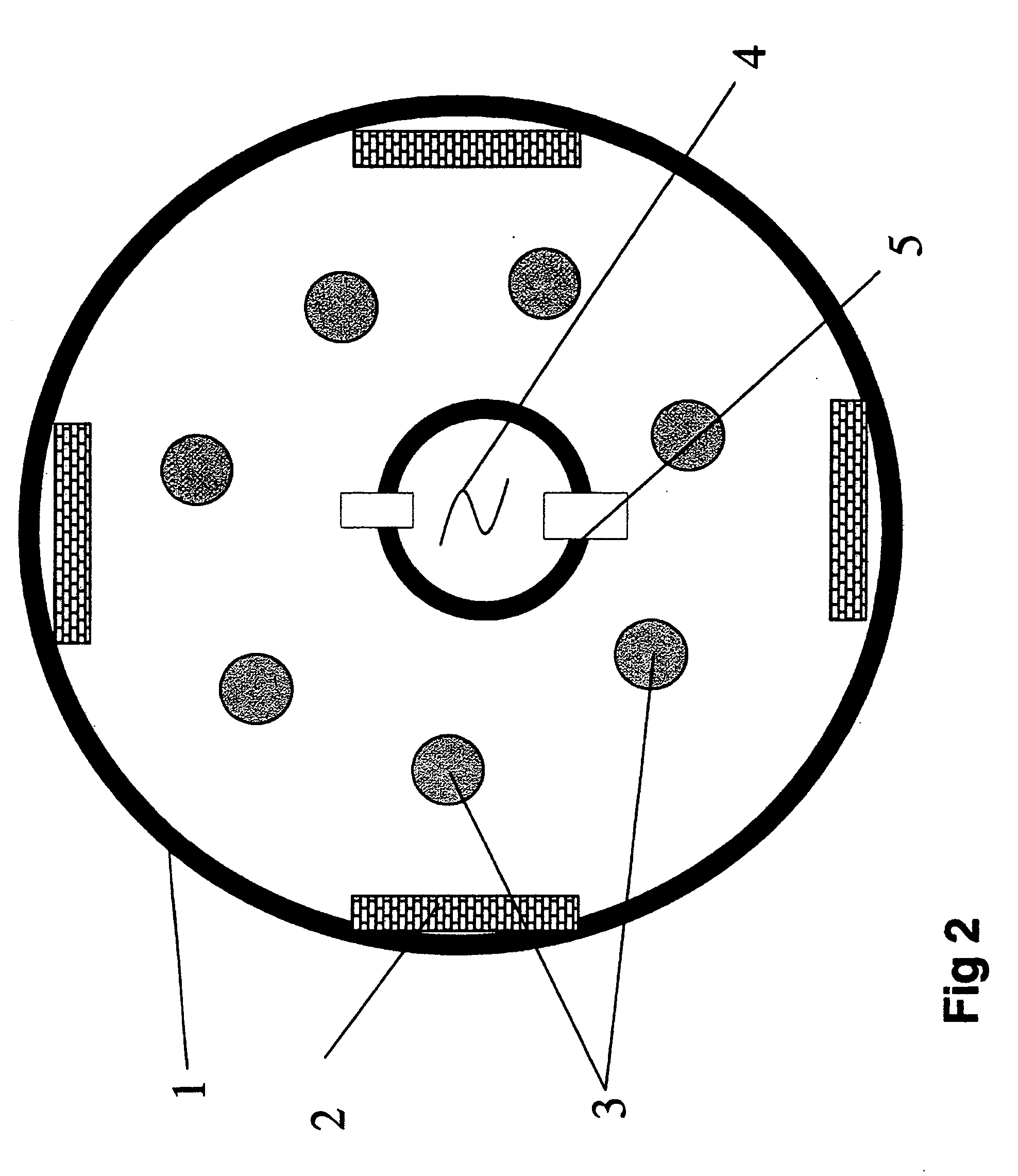
[0029] Example 1 was repeated utilizing the system as described above but with the addition of a centrally situated hot W-filament, as indicated in FIG. 2. By heating the filament with 11 A and applying a voltage of 360 V between the filament (cathode) and the reactor wall (anode), etching was achieved at 0.2 Pa. With a substrate—Ti-counter electrodes (magnetron sources) voltage of 200 V, a substrate current of 7 A was measured. This voltage was not the minimum etching voltage necessary but selected as appropriate. The substrates were clearly more and deeper etched and showed no signs of redeposition, not even on highly shadowed areas.

[0030] Thus, when etching according to the present invention a more efficient etch was obtained, at a lower substrate voltage which implies less impact damage and at a lower pressure thus eliminating redeposition.

example 3

[0031] The inserts from Examples 1 and 2 were, immediately following the etch, coated with a 1.6 μm thick layer of Al2O3 using a standard deposition process: DMS using two pairs of magnetrons equipped with Al targets. A background pressure of 0.23 Pa Ar was maintained for the sputtering gas discharges which were run at 40 kW each. Oxygen reactive gas was fed at 2×30 sccm and controlled by an optical emission feedback circuit. This resulted in crystalline alumina layers. The two sets of inserts were evaluated in a turning test in stainless steel, with the object to determine the adhesion of the coatings. The results indicated that the inserts etched according to prior art technology exhibited extensive flaking while the inserts etched according to the invention showed less flaking and less indications of wear.


PUM

PropertyMeasurementUnit
Plasma poweraaaaaaaaaa

Abstract

The present invention relates to a device for improving plasma activity in a magnetron sputtering reactor containing substrates to be coated where a primary plasma is created by a DC or AC voltage applied between the substrates and an additional electrode. Increased plasma activity is obtained by thermionic emission of electrons from a hot filament heated by either DC or AC current or combinations thereof. The device is particularly useful for increasing the adhesion of layers deposited by magnetron sputtering on cutting tool inserts made of cemented carbide, high speed steels, cermets, ceramics or cubic boron nitride.

Description

BACKGROUND OF THE INVENTION [0001] The present invention relates to a device for achieving an enhanced plasma activity in PVD reactors. Due to the increased plasma density the invention enables operation of sputter etching at much lower pressure than otherwise possible in a magnetron sputtering PVD coating chamber. Thus, gas phase scattering is avoided and problems with redeposition and contamination of sputter cleaned surfaces of 3-D objects are eliminated. The invention allows for sputter etching substrates in a magnetron sputtering system at bias values suitable to avoid impact damage. [0002] Modern high productivity chip forming machining of metals requires reliable tool inserts with high wear resistance, good toughness properties and excellent resistance to plastic deformation. [0003] This has so far been achieved by employing cemented carbide inserts coated with wear resistant layers like TiN, TixAlyN, CrxAlyN and Al2O3. Such layers have been commercially available for many ye...

Claims


Application Information

Patent Timeline
IPC IPC(8): C23C14/00
CPCC23C14/022H01J37/3405H01J37/3233C23C14/355C23C14/3478
Inventor MYRTVEIT, TORILRODMAR, MARKUSSELINDER, TORBJORN
Owner SANDVIK INTELLECTUAL PROPERTY AB
Why Eureka
Try Eureka