Reduced electric field DMOS using self-aligned trench isolation

a self-aligned trench and electric field technology, applied in semiconductor devices, semiconductor/solid-state device details, electrical apparatus, etc., can solve the problems of reducing the switching speed and current carrying capacity of transistors, affecting both cost and reliability, and the manufacturing process is more difficult, so as to reduce the local electric field, reduce capacitance, and improve the isolation voltage

Active Publication Date: 2007-01-25
ATMEL CORP
View PDF6 Cites 31 Cited by
  • Summary
  • Abstract
  • Description
  • Claims
  • Application Information

AI Technical Summary

Benefits of technology

[0014] Due to the aforementioned attributes and processing methods, the present invention is, inter alia, capable of attaining a higher isolation voltage between gate and drift regions than the prior art without degrading a trajectory of injected carriers or forcing them deeper into the body of the device. Also, the structure of the resulting device allows for a greatly reduced capacitance between the device gate and drift region with an elimination of the “gate wrap-around,” thereby reducing a local electric field.

Problems solved by technology

As the number of electronic devices per given area of a silicon wafer increases, manufacturing processes employed become more difficult.
This increased parasitic resistance degrades the switching speed and current carrying capabilities of the transistor.
The necessity of LDD regions also adds process steps to fabrication which negatively affect both cost and reliability.
The wide channel region formed in such a process contributes undesirable characteristics to a transistor's performance.
The gate wrap-around region 115, however, has at least the following detrimental affects to MOS device performance: (1) isolation voltages between gate and drift regions of a device are reduced; and (2) the divot produces a high capacitance region between the gate and drift regions, thereby creating a high local-electric field.

Method used


Image

  • Reduced electric field DMOS using self-aligned trench isolation
  • Reduced electric field DMOS using self-aligned trench isolation
  • Reduced electric field DMOS using self-aligned trench isolation

Examples


Embodiment Construction

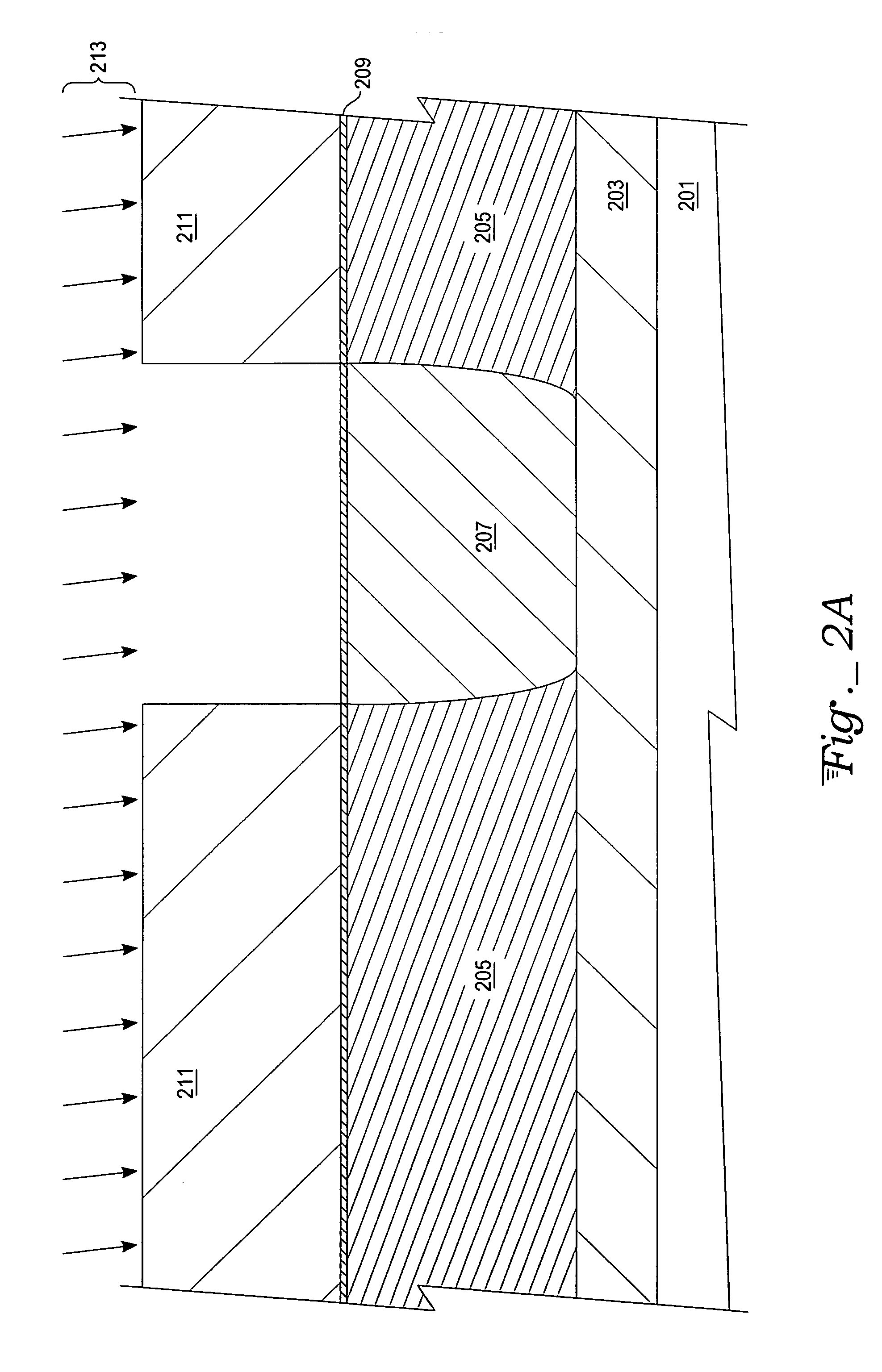
[0018] With reference to FIG. 2A, beginning exemplary processes of the present invention utilize a silicon-on-insulator (SOI) technique and include a substrate 201, an oxide isolation layer 203, and an SOI layer 205. A screen oxide 209 is either thermally grown or deposited on the SOI layer 205. A patterned and etched photoresist layer 211 provides a mask for an ion implantation step. In a specific embodiment, a concentration of boron atoms 213 forms a retrograde p-well 207, thus forming a body for an NMOS device. A skilled artisan will recognize that other doping techniques, such as diffusion, may also be readily employed to produce a similar p-well area.

[0019] In this exemplary embodiment, the substrate 201 is a silicon wafer. Alternatively, the substrate 201 could be another elemental group IV semiconductor or a compound semiconductor (e.g., groups III-V or II-VI). The substrate 201 may alternatively be a non-semiconductor, such as a photomask blank.

[0020] In FIG. 2B, additiona...


PUM


Abstract

A method of fabricating an electronic device and the resulting electronic device. The method includes forming a gate oxide on an uppermost side of a silicon-on-insulator substrate; forming a first polysilicon layer over the gate oxide; and forming a first silicon dioxide layer over the first polysilicon layer. A first silicon nitride layer is then formed over the first silicon dioxide layer followed by a second silicon dioxide layer. Shallow trenches are etched through all preceding dielectric layers and into the SOI substrate. The etched trenches are filled with another dielectric layer (e.g., silicon dioxide) and planarized. Each of the preceding dielectric layers are removed, leaving an uppermost sidewall area of the dielectric layer exposed for contact with a later-applied polysilicon gate area. Formation of the sidewall area assures a full-field oxide thickness thereby producing a device with a reduced-electric field and a reduced capacitance between gate and drift regions.

Description

TECHNICAL FIELD [0001] The invention relates to electronic semiconductor devices and methods of fabrication, and, more particularly, to semiconductor devices and fabrication methods thereof for reducing electric fields and other deleterious effects by using self-aligned trench isolation techniques. BACKGROUND ART [0002] The electronics industry continues to rely upon advances in semiconductor technology to realize higher-functioning devices in more compact areas. For many applications, realizing higher-functioning devices requires integrating a large number of electronic devices into a single silicon die. As the number of electronic devices per given area of a silicon wafer increases, manufacturing processes employed become more difficult. [0003] An important subject of ongoing research in the semiconductor industry is a reduction in the dimensions of devices used in integrated circuits. Planar transistors such as metal oxide semiconductor (MOS) transistors are particularly suited t...

Claims


Application Information

Patent Timeline
Patent Type & Authority Applications(United States)
IPC IPC(8): H01L29/00
CPCH01L21/823481H01L29/0653H01L29/0847H01L29/086H01L29/7835H01L29/66659H01L29/66689H01L29/7824H01L29/42368
Inventor MILLER, GAYLE W. JR.DUDEK, VOLKERGRAF, MICHAEL
Owner ATMEL CORP
Why Eureka
Try Eureka