Method for casting polycrystalline silicon

a polycrystalline silicon and casting technology, applied in the direction of crystal growth process, polycrystalline material growth, chemistry apparatus and processes, etc., can solve the problems of degrading the electrical properties of the solar cell substrate, excessive mixture of oxygen, and increasing the production cost to raise the power generation price, so as to reduce the production cost of the solar energy generation apparatus, the effect of reducing the manufacturing cos

Inactive Publication Date: 2007-02-22
SUMCO CORP
View PDF3 Cites 19 Cited by
  • Summary
  • Abstract
  • Description
  • Claims
  • Application Information

AI Technical Summary

Benefits of technology

[0025] According to the method for casting polycrystalline-silicon by the present invention, in the production of the silicon ingot used for the solar cell, the productivity is largely improved, which allows manufacturing cost to be remarkably reduced. Therefore, the production cost of the solar energy generation apparatus can be decreased.

Problems solved by technology

Because a high grade, less-defect, dislocation-free, single crystal having the same grade as the substrate material of a semiconductor integrated circuit is required in the single crystal used for the solar cell, the solar-cell single crystal is produced by a Czochralski method in which the single crystal is pulled from molten silicon, which causes production cost to be increased to raise power generation price.
However, excessive mixture of oxygen is not desirable because electrical properties of the solar cell substrate are degraded.
However, in the casting method in which the crucible and the mold are used, it is difficult to prevent the impurity contamination caused by bringing silicon into contact with the chamber wall or it is difficult to prevent the mixture of oxygen from the quartz crucible.

Method used


Image

  • Method for casting polycrystalline silicon
  • Method for casting polycrystalline silicon
  • Method for casting polycrystalline silicon

Examples


examples

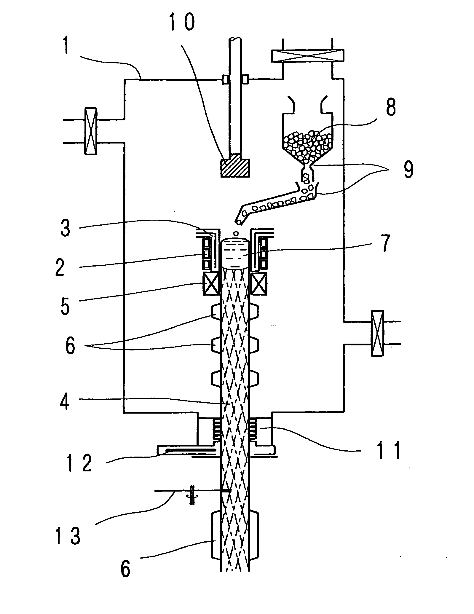
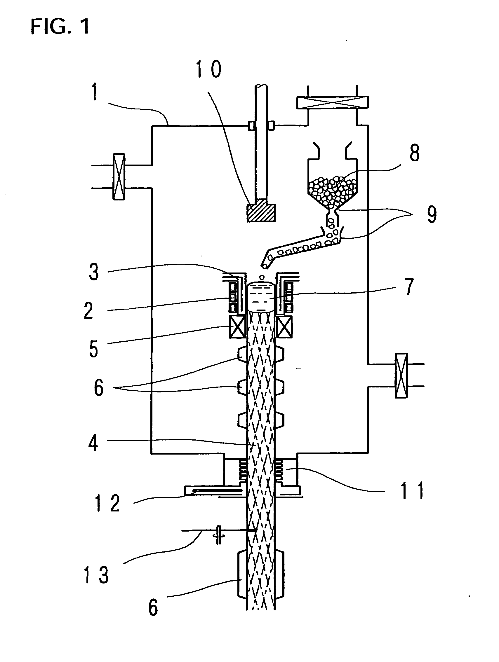
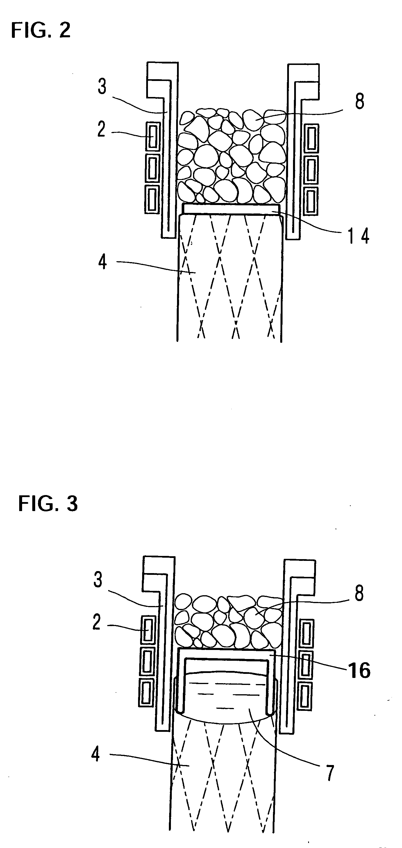
[0046] The polycrystalline silicon ingot was produced with the water-cooled crucible induction melting-casting apparatus whose sectional structure was schematically shown in FIG. 2. The copper water-cooled crucible placed in the heating induction heating coil 2 was configured to be in the square having one side of 170 mm in horizontal section of the inner wall, and the induction heating coil 2 had an effective height of 160 mm.

[0047] A silicon ingot (dummy ingot) having the same sectional shape as the ingot and the length of 200 mm was inserted into the crucible such that lower-end position of the induction heating coil 2 was set at the upper surface of the dummy ingot, and the lump-like silicon of the raw material was charged on the dummy ingot. After the chamber was evacuated to a vacuum, argon gas was introduced to the atmospheric pressure, and the melting got started. Because the heat generation of the initial raw material was insufficient at the beginning of the heating, the c...


PUM

PropertyMeasurementUnit
heightaaaaaaaaaa
heightaaaaaaaaaa
lengthaaaaaaaaaa

Abstract

In melting and casting by a water-cooled crucible induction melting technique, a partition means is inserted on top portion of a melt, and a new raw material for is charged on an upper side of the partition means to continue the melting and casting. Therefore, the continuous casting can be kept while avoiding mixture of the melt on a lower side of with the melt on an upper side of the partition means. A partition plate or a partition plate with legs can be used as the partition means. When the present invention is applied to production of a silicon ingot used for a solar cell and the like, productivity is largely improved, which allows costs to be remarkably reduced in solar energy generation. Therefore, the present invention can widely be utilized as the method for casting a polycrystalline-silicon ingot for a solar cell.

Description

FIELD OF THE INVENTION [0001] The present invention relates to a method for casting polycrystalline silicon in which an ingot is continuously produced to be used for a solar cell substrate. DESCRIPTION OF THE RELATED ART [0002] A silicon crystal is used as a substrate material in most (at least 90%) of the currently produced solar cells. The silicon crystal includes a single crystal and a polycrystal. Generally the solar cell having high conversion efficiency can be obtained by using the single crystal as the substrate, when light energy incident to the solar cell is converted into electrical energy. [0003] Because a high grade, less-defect, dislocation-free, single crystal having the same grade as the substrate material of a semiconductor integrated circuit is required in the single crystal used for the solar cell, the solar-cell single crystal is produced by a Czochralski method in which the single crystal is pulled from molten silicon, which causes production cost to be increased...

Claims


Application Information

Patent Timeline
Patent Type & Authority Applications(United States)
IPC IPC(8): C30B11/00C30B17/00C30B21/02C30B28/06C30B9/00
CPCB22D11/086C30B11/001C30B11/002C30B11/003B22D11/141B22D11/001B22D11/0401B22D11/126C30B29/06
Inventor KANEKO, KYOJIRO
Owner SUMCO CORP
Why Eureka
Try Eureka