
Process for producing semiconductor nanocrystal cores, core-shell, core-buffer-shell, and multiple layer systems in a non-coordinating solvent utilizing in situ surfactant generation

a technology of in situ surfactant and semiconductor nanocrystals, which is applied in the direction of antimony organic compounds, group 3/13 element organic compounds, antimony organic compounds, etc., can solve the problems of affecting the optical properties of the desired iii-v nanocrystal, and properties that have the potential to mask or obscure the optical properties of the desired nanocrystals. , to redu

Inactive Publication Date: 2007-03-01
THE RES FOUND OF STATE UNIV OF NEW YORK
View PDF12 Cites 27 Cited by
  • Summary
  • Abstract
  • Description
  • Claims
  • Application Information

AI Technical Summary

Benefits of technology

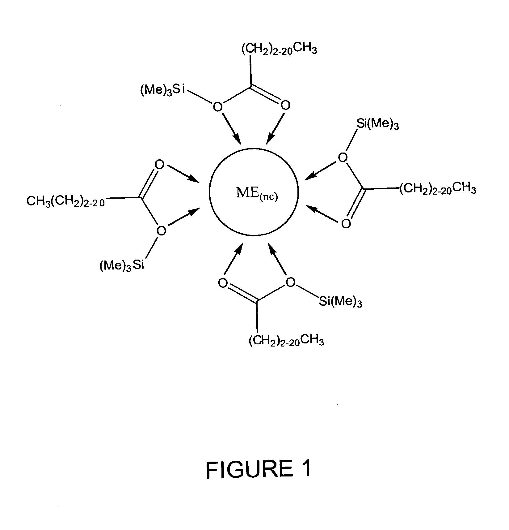
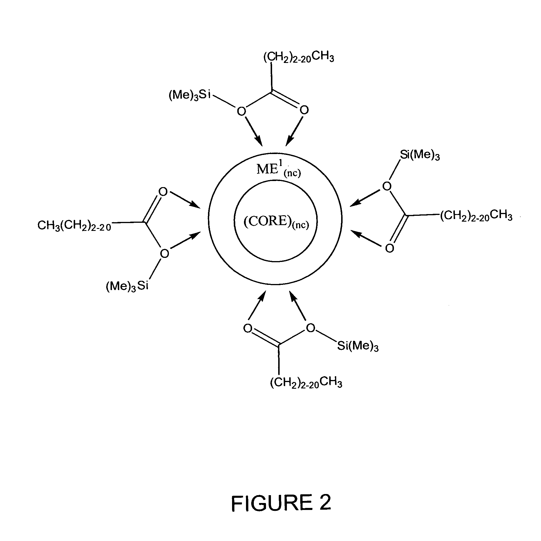
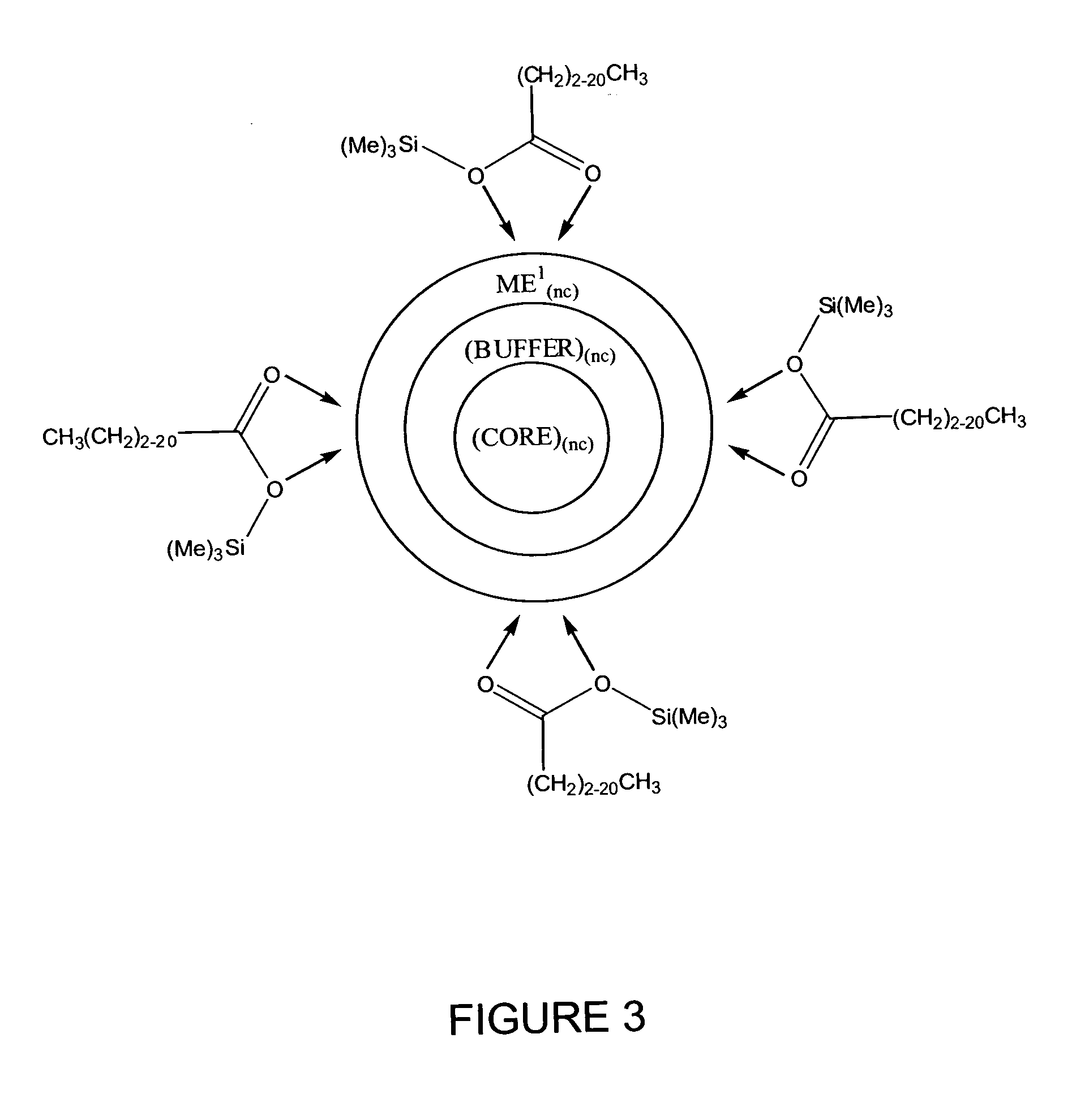
[0024] The present invention affords the reliable and reproducible preparation of high quality nanocrystals, in particular, semiconductor nanocrystals, in near monodispersity at low reaction temperatures in significantly shorter times (e.g., 1-24 hours at 270° C. for III-V semiconductor nanocrystals) than existing technologies. The present invention also allows for the rapid synthesis of nanocrystals having multiple layers of III-V or II-VI material, such as, for example, core-shell, core-buffer-shell, or other multiple layer systems. The nanocrystals are prepared in non-coordinating solvents without the necessity of any added surfactant, ligand and / or coordinating solvent. The shell materials can be synthesized rapidly, with size-control, at low temperatures (e.g., <200° C.). The shell preparation allows for excellent surface passivation resulting in a dramatic increase in the quantum efficiency of the core particles. In multiple layer systems, each layer can be tuned to give the desired optical properties depending on the individual layer composition and size. The individual layers of the nanocrystals may be formed of the same III-V or II-VI materials, or any combination thereof. For example, the core may be any III-V or II-VI material, a second layer may be any III-V or II-VI material, a third layer may be any III-V or II-VI material, etc. As such, the resultant nanocrystals are dispersible in common solvents, allowing for many uses. The nanocrystals may be used, for example, for microelectronics, for photovoltaics, for bioimaging, for incorporation in different solid matrices using sol-gel processed glass and polymers, and for making binary as well as ternary and quaternary systems.
[0026] The processes of the present invention solve the problems of traditional methods by rapid generation of III-V or II-VI nanocrystals (minutes) with concomitant formation of a surface capping material (through in situ surfactant generation). The rapidity of the reaction reduces the time required at elevated temperatures, thereby drastically reducing or eliminating the decomposition products associated with traditional preparative methods. The processes of the present invention permit very reproducible preparation of III-V and II-VI nanocrystals with excellent size control and yields nanocrystals whose surface modification is easily afforded. The new preparative route offers the potential to be scaled to commercial capacities.
[0027] The processes of the present invention directed to preparative routes to core-shell, core-buffer-shell, and other multiple layer nanocrystals, improve upon traditional methods of producing these types of particles by avoiding the use of elaborate, and possibly detrimental, surfactants or coordinating solvents. The processes are also considerably faster, leading to much less expensive and easily scalable synthesis of these highly luminescent particles.

Problems solved by technology

Decomposition products resulting from these methods have been shown to possess optical properties which have the potential to interfere with the optical properties of the desired III-V nanocrystals.
Moreover, the III-V semiconductor nanocrystals prepared by these methods are generally polydispersed (1-20 nm) and the results are somewhat erratic or irreproducible.
An added disadvantage is that when any of the commonly utilized surfactants are exposed to high temperatures (>100° C.
), their optical properties also have the potential to mask or obscure the optical properties of the desired nanocrystals.
However, although both of these methods are excellent techniques for the preparation of thin film or bulk III-V semiconductor materials, neither technique is capable of producing monodispersed III-V semiconductor nanocrystals and neither offers control or exchange of the surface capping material which would allow incorporation of the semiconductor nanocrystals into desired host matrices.
Also, these traditional preparative routes generally require long reaction times at high temperatures with most of these approaches utilizing very dangerous and reactive metal precursors (i.e., CdMe2 and ZnEt2).
These impurities hinder the desired electronic or optical properties of the nanocrystals.

Method used


Image

  • Process for producing semiconductor nanocrystal cores, core-shell, core-buffer-shell, and multiple layer systems in a non-coordinating solvent utilizing in situ surfactant generation
  • Process for producing semiconductor nanocrystal cores, core-shell, core-buffer-shell, and multiple layer systems in a non-coordinating solvent utilizing in situ surfactant generation
  • Process for producing semiconductor nanocrystal cores, core-shell, core-buffer-shell, and multiple layer systems in a non-coordinating solvent utilizing in situ surfactant generation

Examples


example 1

Synthesis of Group III Precursors through Cyclopentadiene Elimination

[0064] The following describes the preparation of very pure Group III precursors which do not contain halide impurities and which do not require the addition of coordinating solvents and / or surfactants for subsequent preparation of semiconductor nanocrystals. Direct synthesis of a series of very pure compounds of the general formula M(ERx)3 is illustrated in Scheme 1.

[0065] Even though these complexes might be synthesized directly via the elimination of methane, ethane or neopentane from MMe3, MEt3 or M(CH2CMe3)3, respectively, each subsequent elimination of an alkane molecule requires additional time and subsequently higher temperatures, and the isolation of pure M(ERx)3 complexes becomes very, very difficult. The direct synthesis of M(ERx)3 from In(C5H5)3 and Ga(C5H5)3 was conducted according to Scheme 1 at room temperature in less than 4 hours.

[0066] Table 1 provides examples of compounds of general formula ...

example 2

Synthesis of In(Myristate)3

[0068] A 500 mL three-neck round bottom flask was loaded with 3.4358 grams of In(C5H5)3 (11.08 mmoles), 7.6164 grams of Myristic Acid (33.35 mmoles, 3.01 mol equivalents), a stir bar, and equipped with a glass stopper in one-neck, a medium grain scintered frit which has a 300 mL one-neck round bottom connected via a 24 / 40 ground glass joint and a high-vacuum line adapter. After removal from the glove box, the entire apparatus was connected to the high-vacuum line where approximately 100-150 mL of dry benzene is distilled into the reaction vessel. The benzene was rapidly thawed using warm water and the reaction was stirred for 3-4 hours at room temperature. Next, all of the volatile components were removed by flask to flask distillation and approximately 75-100 mL of dry ether was distilled onto the crude reaction product. Then the sample was filtered through the flit and the volatile ether distilled back onto the product, this process was repeated for thr...

example 3

Synthesis of In(Laurate)3

[0069] The procedure described in the synthesis of In(Myristate)3 was followed, and 2.0968 g In(C5H5)3 (6.76 mmoles) and 4.1642 g Lauric Acid (20.8 mmoles, 3.08 eq) were used. Yield 3.0469 In(Laurate)3, 63.24%. Anal. Calcd for C36H69InO6: C, 60.66; H, 9.76. Found: C, 58.2; H, 10.5. 1H NMR (d6-benzene) T 55° C.: δ 7.15 (benzene), δ 2.59 (br, 2H), δ 1.78 (q, J 7.0 Hz, 2H), δ 1.32 (br, 16H), δ 0.924 (t, J 6.2 Hz, 3H). For comparison Lauric Acid 1H NMR (d6-Benzene) RT: δ 12.72 (br, 1H), δ 7.15 (benzene), δ 2.08 (t, J 7.6 Hz, 2H), δ 1.47 (q, J 7.0 Hz, 2H), δ 1.25-1.13 (br-m, 16H), δ 0.91 (t, J 6.8 Hz, 3H).


PUM


Abstract

A process for producing semiconductor nanocrystal cores, core-shell, core-buffer-shell, and multiple layer systems is disclosed. The process involves a non-coordinating solvent and in situ surfactant generation.

Description

[0001] This application claims the benefit of U.S. Provisional Patent Application Ser. No. 60 / 456,384, filed Mar. 20, 2003, which is hereby incorporated by reference in its entirety.[0002] This invention arose out of research sponsored by the U.S. Air Force Office of Scientific Research (AFOSR Grant No. F496200110358) The U.S. Government may have certain rights in this invention.FIELD OF THE INVENTION [0003] This invention relates to a process for producing III-V or II-VI nanocrystals, core-shell, core-buffer-shell, and multiple layer systems. BACKGROUND OF THE INVENTION [0004] There is considerable interest in processes for the preparation of semiconductor nanocrystals, the applications for which include, for example, optical communications, photonic chips, photovoltaic devices, and biolabels for bioimaging. Traditional preparative routes to III-V semiconductor nanocrystals require the use of coordination solvents such as trioctylphosphine oxide (“TOPO”) or dodecylamine (“DA”) and ...

Claims


Application Information

Patent Timeline
IPC IPC(8): C07F5/00C07F7/18C07F9/00C07F5/06C07F9/02C30B7/00H01S
CPCC30B7/00C30B29/40C30B7/005C30B29/60C30B29/46
Inventor LUCEY, DERRICK W.MACRAE, DAVID J.PRASAD, PARAS N.BEACHLEY, ORVILLE T. JR.
Owner THE RES FOUND OF STATE UNIV OF NEW YORK
Learn More