Display device and method for manufacturing the same, and television receiver

a technology for television receivers and display panels, which is applied in the direction of basic electric elements, semiconductor devices, electrical equipment, etc., can solve the problems of waste of material costs, forced discharge of large quantities of effluent, and difficulty in manufacturing a display panel at good productivity by low cost in a conventional patterning method, so as to improve the utilization efficiency of materials and simplify the manufacturing step.

Inactive Publication Date: 2007-03-08
SEMICON ENERGY LAB CO LTD
View PDF16 Cites 44 Cited by
  • Summary
  • Abstract
  • Description
  • Claims
  • Application Information

AI Technical Summary

Benefits of technology

[0020] According to the invention, the gate electrode or the wiring is formed with a droplet discharge method, and a conductive material can be formed of Ag or an alloy containing Ag. In addition, a silicon nitride film or a silicon nitride oxide film is provided over the gate electrode or an upper layer of the wiring by being in contact; therefore, the gate electrode can be prevented from being deteriorated due to oxidization.
[0021] In the invention, it is also possible that the semiconductor layer, which is a main portion of a TFT, contains hydrogen and halogen, and is formed from a semi-amorphous semiconductor containing a crystal structure. Accordingly,...

Problems solved by technology

A large sized glass substrate is effective in enlarging an area and increasing the number of a display panel to be obtained; however, it is difficult to manufacture a display panel at good productivity by low cost in a conventional patterning method.
Moreover,...

Method used


Image

  • Display device and method for manufacturing the same, and television receiver
  • Display device and method for manufacturing the same, and television receiver
  • Display device and method for manufacturing the same, and television receiver

Examples


embodiment mode 1

[0064] A method for manufacturing a channel protective type TFT and a display device with the use thereof are explained in Embodiment mode 1.

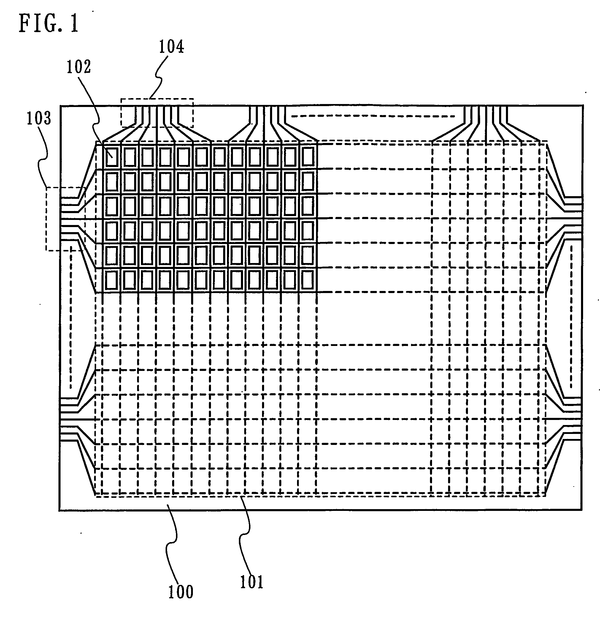
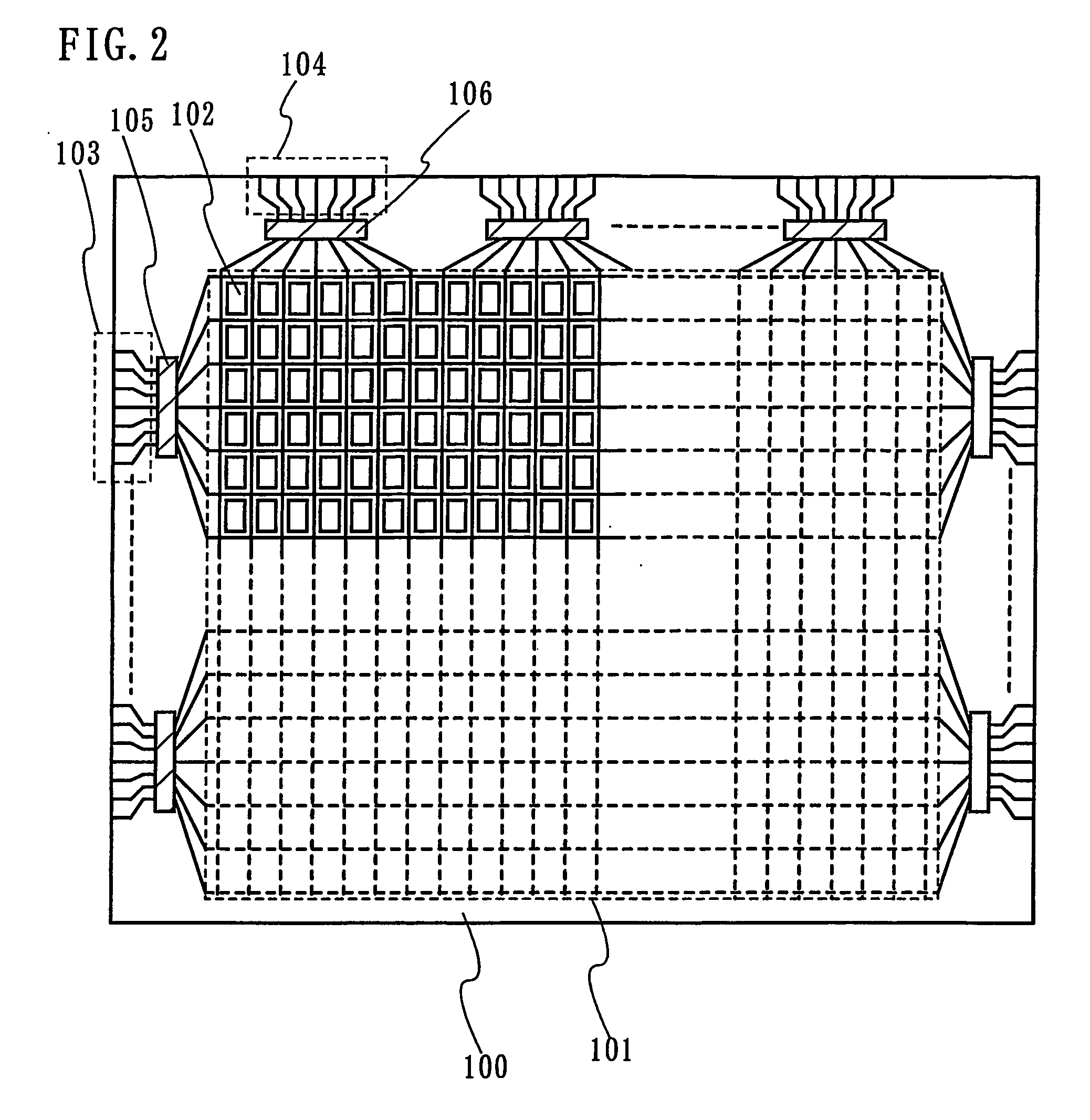
[0065]FIG. 4A shows a step of forming a gate electrode, and a gate wiring and a capacitor wiring connected to the gate electrode over a substrate 100 with a droplet discharge method. Note that FIG. 4A shows a longitudinal sectional structure, and FIG. 8 shows a planar structure corresponding to A-B and C-D thereof.

[0066] In addition to a non-alkaline glass substrate such as barium borosilicate glass, alumino borosilicate glass, or aluminosilicate glass manufactured with a fusion method or a floating method, and a ceramic substrate, a plastic substrate having the heat resistance that can withstand processing temperature or the like can be used for the substrate 100. In addition, a semiconductor substrate such as single crystal silicon, a substrate in which a surface of a metal substrate such as stainless is provided with an insulating layer ma...

embodiment mode 2

[0102] A method for manufacturing a channel etch type TFT and a display device with the use thereof are explained in Embodiment Mode 2.

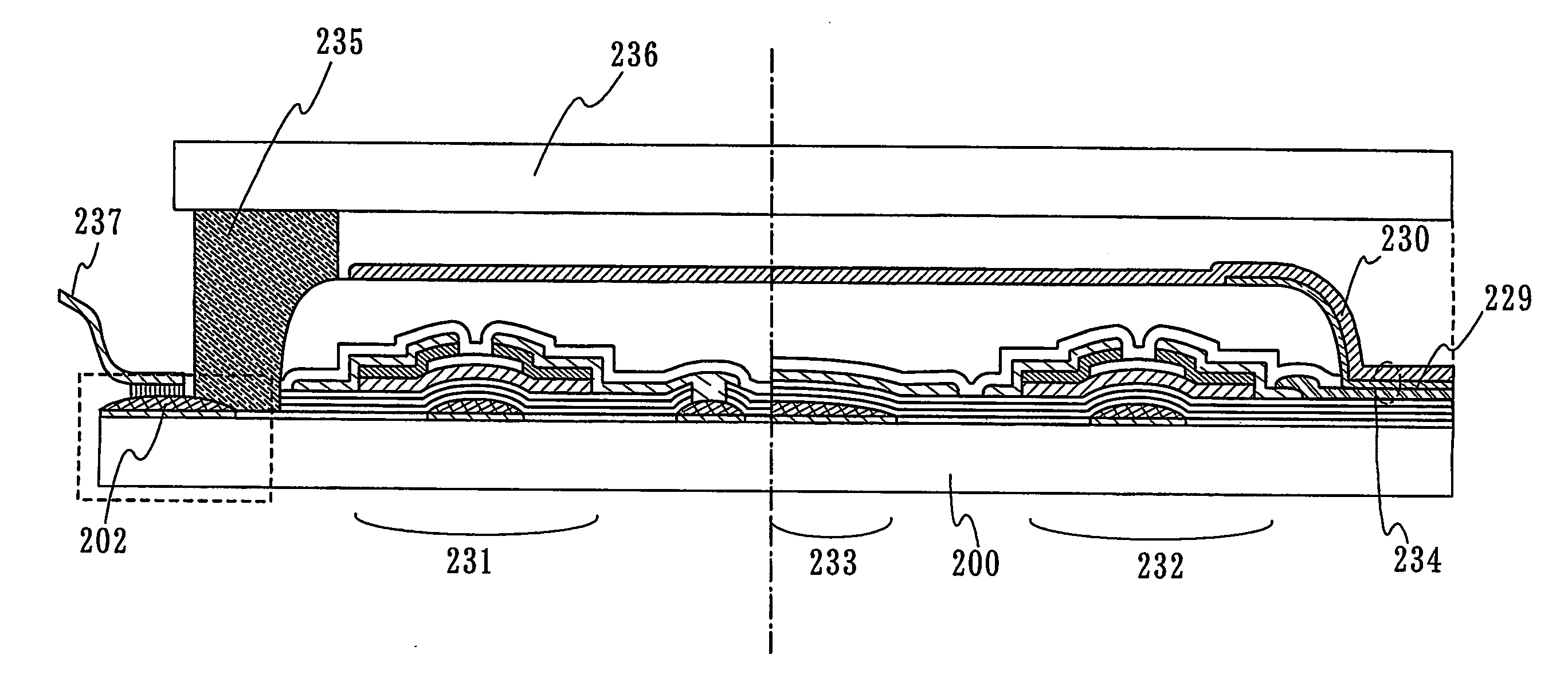
[0103] A gate wiring 202, a gate electrode 203, a capacitor electrode 204, and a gate electrode 205 are formed over a substrate 100 by discharging a composition containing a conductive material by a droplet discharge method. Next, a gate insulating layer 207 is formed to have a single layer structure or a laminated structure by a plasma CVD method or a sputtering method. The gate insulating layer 207 may be formed from silicon nitride or silicon oxide in the same manner as Embodiment Mode 1. Furthermore, a semiconductor layer 211 functioning as an active layer is formed. The above-mentioned steps are the same as those in Embodiment Mode 1.

[0104] An n-type semiconductor layer 215 is formed on the semiconductor layer 211 (see FIG. 12A). Next, a mask 302 is formed by selectively discharging a resist composition on the n-type semiconductor layer 215. S...

embodiment mode 3

[0108] In an EL display panels manufactured by Embodiment Mode 1 and Embodiment Mode 2, as explained in FIG. 3, a scanning line driver circuit can be formed on a substrate 100 by forming a semiconductor layer from an SAS.

[0109]FIG. 22 shows a block diagram of the scanning line driver circuit composed of n-channel type TFTs using the SAS in which electric field effect mobility of from 1 cm2 / V·sec to 15 cm2 / V·sec is obtained.

[0110] In FIG. 22, a pulse output circuit 500 is a circuit outputting a sampling pulse for one stage and includes a shift register. The pulse output circuit 500 is connected to a buffer circuit 501 and connected to a pixel 502 (corresponds to a pixel 102 in FIG. 3) at the end thereof.

[0111]FIG. 23 shows a specific structure of the pulse output circuit 500, and this pulse output circuit 500 is composed of n-channel type TFTs 601 to 613. The size of the TFTs may be decided by the pulse output circuit 500 in consideration of an operating characteristic of the n-ch...


PUM


Abstract

According to the present invention, which is a display device in which a light-emitting element where an organic substance generating luminescence referred to as electroluminescence or a medium including a mixture of an organic substance and an inorganic substance is sandwiched between electrodes is connected to a TFT, the invention is to manufacture a display panel by forming at least one or more of a conductive layer which forms a wiring or an electrode and a pattern necessary for manufacturing a display panel such as a mask layer for forming a predetermined pattern is formed by a method capable of selectively forming a pattern. A droplet discharge method capable of forming a predetermined pattern by selectively discharging a droplet of a composition in accordance with a particular object and by forming a conductive layer or an insulating layer is used as a method capable of selectively forming a pattern.

Description

TECHNICAL FIELD [0001] The present invention relates to a display device to which an active element such as a transistor formed over a glass substrate is applied and to a method for manufacturing the same. BACKGROUND ART [0002] Conventionally, a display panel of a so-called active matrix driving method constituted by a thin film transistor (hereinafter also referred to as a “TFT”) over a glass substrate is known. As well as a manufacturing technique of a semiconductor integrated circuit, this display panel needs a step of patterning a thin film such as a conductor, a semiconductor, or an insulator due to a light-exposure step using a photomask. [0003] A size of a mother glass substrate used for manufacturing a display panel is enlarged from 300 mm×400 mm of the first generation in the early 1990s to 680 mm×880 mm or 730 mm×920 mm of the fourth generation in 2000. Furthermore, the manufacturing technique made such a development that a number of display panels can be obtained from one...

Claims


Application Information

Patent Timeline
IPC IPC(8): H01L29/04H01L21/336H01L21/77H01L21/84H01L27/12H01L27/32H01L51/56
CPCH01L27/12H01L27/3276H01L27/1292H01L29/66765H01L51/56H01L29/66757H10K59/131H10K71/00H01L21/28132H10K50/805H10K50/84H10K50/30H10K2102/302
Inventor YAMAZAKI, SHUNPEIMAEKAWA, SHINJIFURUNO, MAKOTONAKAMURA, OSAMUIMAI, KEITARO
Owner SEMICON ENERGY LAB CO LTD
Why Eureka
Try Eureka