III-nitride current control device and method of manufacture

a current control device and nitride technology, applied in the direction of semiconductor devices, basic electric elements, electrical apparatus, etc., can solve the problems of limited applicability to power management limited thickness of strained algan/gan systems, etc., to achieve high current densities with low resistive losses, low leakage, and high breakdown field

Inactive Publication Date: 2007-03-22
INFINEON TECH AMERICAS CORP
View PDF16 Cites 34 Cited by
  • Summary
  • Abstract
  • Description
  • Claims
  • Application Information

AI Technical Summary

Benefits of technology

[0019] According to a feature of the present invention, the schottky contact is formed in a recess of a III-nitride layer, such that the device is non-conducting until a forward voltage is applied. Advantageously, recess has sloped walls to permit easy controllability of device parameters.
[0021] In accordance with another feature of the present invention, the pinch resistor device can be tuned to obtain unbalanced current limiting features, similar to a rectifier, as well as varying ON resistance. The device can also be tailored to have a high current carrying capacity in both directions.
[0022] According to another embodiment of the present invention, there is provided a schottky type rectifier in a III-nitride material system, where the device conducts current through a channel that includes a 2DEG formed by the interface of two different layers of III-nitride materials. The device includes a schottky contact and an ohmic contact for conduction in one direction toward the ohmic contact, and a blocking voltage in the other direction toward the schottky contact. The voltage applied to the schottky contact permits current to flow through the channel formed by the 2DEG and out of the ohmic contact, while a voltage applied in an opposite direction depletes the 2DEG under the schottky contact to block voltage during reverse bias. The highly resistive nature of a GaN layer prevents leakage currents through the device, when GaN is used as one of the III-nitride layers. The device may be constructed with little or no doping of the III-nitride layers to obtain a low field during reverse bias that permits high standoff voltages. This attractive feature is obtained without sacrificing an increase in forward bias resistance.
[0025] According to a feature of the present invention, a good GaN insulator interface is provided to improve current carrying capacity, rather than additional insulator layers or structures at the active layer. Without added insulation layers, the epitaxial nature of the hetero-interface described here leads to an order of magnitude higher mobility for the electrons in the 2DEG when accumulated.
[0029] III-nitride current control heterojunction devices can take advantage of symmetrical properties to permit the fabrication of a nominally off device that can block voltage in both directions without sacrificing wafer area. Because of this advantage over traditional devices that block voltage in a single direction, one bi-directional device can replace a number of single directional devices.
[0030] The device is also characterized by low leakage in the contacts and a high breakdown field from the barrier layer. As a result, the device provides a larger dielectric constant compared to conventional insulators such as SiO2 and SiN. The high critical fields of the GaN material allow thin layers to withstand large voltages without dielectric breakdown. The dielectric constant of GaN materials is approximately 10, which is a factor of 2.5 times better than SiO2.

Problems solved by technology

The nominally on nature of the HEMT devices previously fabricated have limited their applicability to power management.
The limitations of nominally on power devices is observed in the need to have a control circuit be powered and operational, before power can be safely controlled by a III-nitride HEMT device.
A drawback of III-nitride HEMT devices that permit high current densities with low resistive losses is the limited thickness that can be achieved in the strained AlGaN / GaN system.
The difference in the lattice structures of these types of materials produces a strain that can result in dislocation of films grown to produce the different layers.
This results in high levels of leakage through a barrier layer, for example.
However, the problem of limited thickness is not addressed by these designs.
While additional insulator layers can permit thicker strained AlGaN / GaN systems to be constructed, the confinement layer produced by the additional insulator results in lower current carrying capacity due to the scattering effect produced on electrons at the GaN / insulator interface.
Also, the additional interface between the AlGaN layer and the insulator results in the production of interface trap states that slow the response of the device.
These devices, however, typically have lower current carrying capacity due to scattering at the GaN / insulator interface.
However, forming gallium nitride materials on silicon substrates to produce semiconductor devices presents challenges that arise from differences in the lattice constant, thermal expansion and bandgap between silicon and gallium nitride.
The problems attendant with the lattice mismatch between GaN and traditional substrate materials are also prevalent in material layer structures involving GaN and GaN alloys.
This type of conventional synchronous rectifier is often used in power applications to avoid the drawbacks of diodes used as rectifiers, such as a forward voltage drop that reduces power efficiency and may also contribute to thermal operating issues.
However, these types of devices are often imprecise due to processing techniques used during their manufacturing.
In conventional devices, the current values that can be carried in pinch resistors is relatively low, so that power applications tend to be somewhat complicated.

Method used


Image

  • III-nitride current control device and method of manufacture
  • III-nitride current control device and method of manufacture
  • III-nitride current control device and method of manufacture

Examples


Embodiment Construction

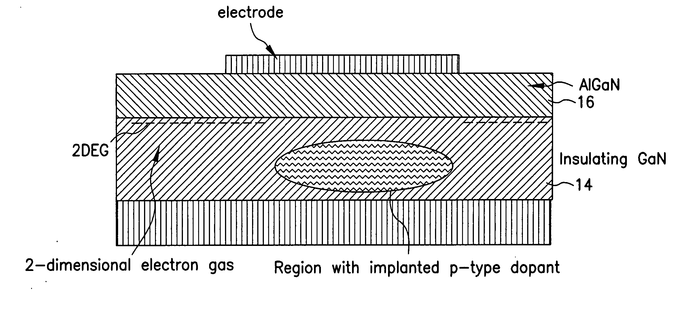
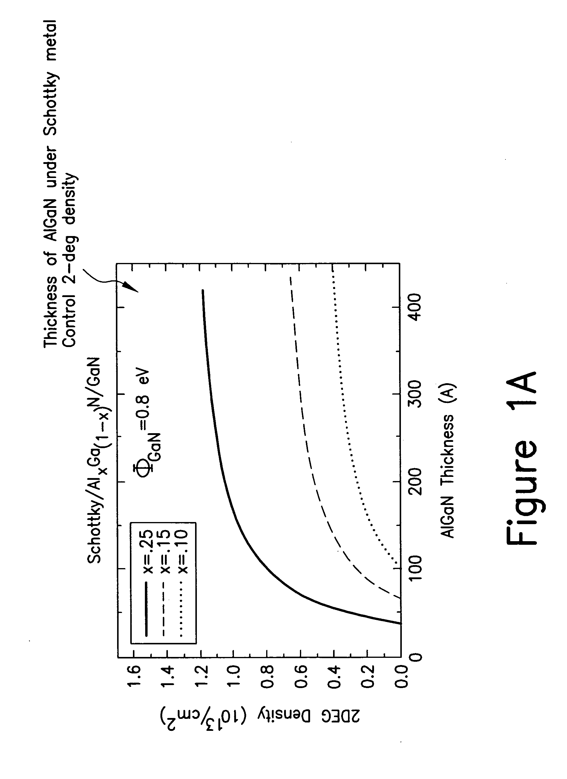
[0049] In the construction of GaN material devices, a number of factors come into play to impact the functionality and capability of the devices. A large lattice mismatch in III-nitride materials and the strong piezoelectric and polarization effects in these materials significantly impact the electrical properties of III-nitride heterojunction devices. A significant number of reported GaN-based devices to date use strained GaN-AlGaN junctions with alloy compositions that are designed to maximize the strain but avoid surpassing the relaxation limit that would lead to dislocations or long term instabilities in the devices. The devices generally are grown to maximize the strain within the limit of relaxation. As the thickness of AlGaN increases, or the Al content in AlGaN increases, the strain also increases which leads to the increase of the 2DEG density, as well as the carrier mobility. However, if the AlGaN layer is increased in thickness too much, or the Al content is too great, th...


PUM


Abstract

A III-nitride device includes a recessed electrode to produce a nominally off, or an enhancement mode, device. By providing a recessed electrode, a conduction channel formed at the interface of two III-nitride materials is interrupted when the electrode contact is inactive to prevent current flow in the device. The electrode can be a schottky contact or an insulated metal contact. Two ohmic contacts can be provided to form a rectifier device with nominally off characteristics. The recesses formed with the electrode can have sloped sides. The electrode can be formed in a number of geometries in conjunction with current carrying electrodes of the device. A nominally on device, or pinch resistor, is formed when the electrode is not recessed. A diode is also formed by providing non-recessed ohmic and schottky contacts through an insulator to an AlGaN layer.

Description

CROSS-REFERENCE TO RELATED APPLICATIONS [0001] The present application is a divisional of U.S. patent application Ser. No. 11 / 040,312, filed Jan. 21, 2005, entitled III-NITRIDE CURRENT CONTROL DEVICE AND METHOD OF MANUFACTURE which is based on and claims the benefit of U.S. Provisional Application Ser. No. 60 / 538,941, filed Jan. 23, 2004, entitled CLAMPED IMPEDANCE FIELD EFFECT RECTIFIER, 60 / 538,864, filed Jan. 23, 2004, entitled III-NITRIDE PIEZOELECTRIC HETEROJUNCTION INTERDIGITATED RECTIFIER, and 60 / 538,794, filed Jan. 23, 2004, entitled III-NITRIDE PINCH RESISTOR, to all of which a claim of priority is hereby made and the disclosure of which is incorporated by reference.BACKGROUND OF THE INVENTION [0002] 1. Field of the Invention [0003] The present invention relates generally to a class of field effect current control devices, and relates more particularly to rectifiers and current limiting devices constructed in the III-Nitride material system. [0004] 2. Description of Related ...

Claims


Application Information

Patent Timeline
Patent Type & Authority Applications(United States)
IPC IPC(8): H01L21/336H01L21/335H01L29/20H01L29/423H01L29/778H01L29/872H01L31/0328H01L31/0336
CPCH01L29/2003H01L29/42316H01L29/872H01L29/7787H01L29/66462H01L29/0623H01L29/737
Inventor BEACH, ROBERT
Owner INFINEON TECH AMERICAS CORP
Why Eureka
Try Eureka