

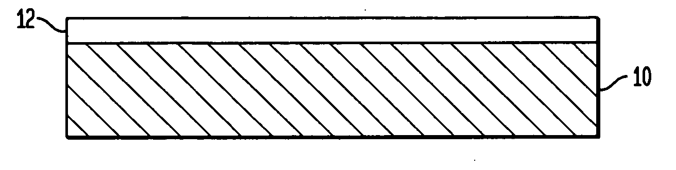
Ge-based semiconductor structure fabricated using a non-oxygen chalcogen passivation step
a technology of chalcogen and passivation step, which is applied in the direction of semiconductor devices, basic electric elements, electrical apparatus, etc., can solve the problems of difficult to obtain a stable gate dielectric, unstable gate dielectric, and the less effective surface passivation technique on ge, so as to reduce the effect of unwanted diffusion or reaction, reducing cost, and improving electrical properties
- Summary
- Abstract
- Description
- Claims
- Application Information
AI Technical Summary
Benefits of technology
Problems solved by technology
Method used
Image

Examples
example
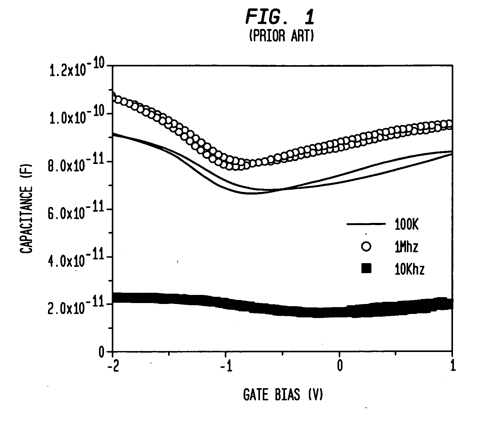
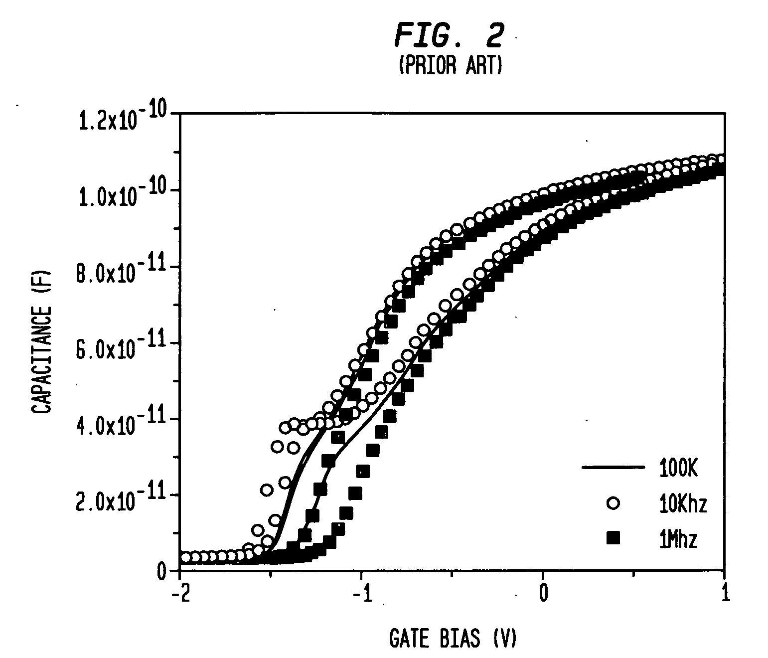
[0062] In this example, a MOS capacitor in which a Ge-containing material was first passivated with sulfur and thereafter a HfO2 dielectric was deposited on the sulfur surface passivated Ge-containing material was prepared. Specifically, the MOS capacitor was prepared by first providing an epi-ready n-Ge (100) material. The surface of the Ge material was then subjected to a wet-chemical precleaning process that included degreasing the surface of the Ge material using an acetone / methanol mixture, treating the degreased surface with a 5:1 H2SO4:H2O treatment for 2 minutes, rinsing in DI water, and etching the Ge surface with 10% HF (aq) for 10 minutes. Following this wet-chemical precleaning process, the Ge-containing material was sulfur passivated utilizing a 50% (NH4)2S (aq) treatment at a temperature between 70°-80° C. for 10 minutes. Following the sulfur passivation, the Ge material was subjected to rinsing in water and then the material was dried by blowing N2 over the sulfur-pas...
PUM
 Abstract
Description
Claims
Application Information