Nanoparticle structure and manufacturing process of multi-wavelength light emitting device

a technology of nanoparticles and light emitting devices, applied in the direction of discharge tubes/lamp details, discharge tubes luminescent compositions, discharge tubes/lamp details, etc., can solve the problems of non-applicability of white light generated by complementary dichroism for full color display of objects, problems to be solved, bluish in the center and yellowish in the periphery, etc., to effectively reduce non-radioactive recombination, effectively elevate the light emitting efficiency of led

Inactive Publication Date: 2007-05-17
NAT CHIAO TUNG UNIV
View PDF7 Cites 63 Cited by
  • Summary
  • Abstract
  • Description
  • Claims
  • Application Information

AI Technical Summary

Benefits of technology

[0011] order to effectively reduce non-radioactive recombination caused by dislocations inside quantum well, and to elevate light emitting efficiency of LED, the present invention provides a growing process of nanoparticle structure; in particular high density of nanoparticles, in multi-stacked active layer to effectively elevate light emitting efficiency of LED.

Problems solved by technology

However, the white light generated by complementary dichroism is not applicable for full color displaying of objects due to the poor color rendering.
Although white light emitting diodes made of blue chips and yellow phosphor particles are well developed currently, there are problems to be solved.
Firstly, emitting wavelength shifting and intensity variation of blue chips and phosphor coating thickness influence the homogeneity of white light, since color combination is essentially dominated by blue light chips (which normally results in bluish in the center and yellowish in the periphery).
In addition, problems relating to high color temperature and low color rendering cause international major manufacturers to develop other methods for manufacturing white light emitting diodes.
However, issues like effective promotion of light emitting efficiency of UV LED, development of UV resistant packing materials, combination of wavelength bands, and environmental contamination of the phosphors need to be solved for it future development.
However, since no proper lattice-matched substrate 1 has been found for current blue and green light emitting diodes with III-nitride as film material, dislocation with density as high as 108˜109 cm−2 has occurred.
The dislocations normally penetrate through quantum well active layer and result in non-radioactive recombination centers therein to reduce internal quantum efficiency, which lowers light emitting efficiency of LED.

Method used


Image

  • Nanoparticle structure and manufacturing process of multi-wavelength light emitting device
  • Nanoparticle structure and manufacturing process of multi-wavelength light emitting device
  • Nanoparticle structure and manufacturing process of multi-wavelength light emitting device

Examples


example 1

Single-Wavelength LED Using Nanoparticle-Containing Active Layer

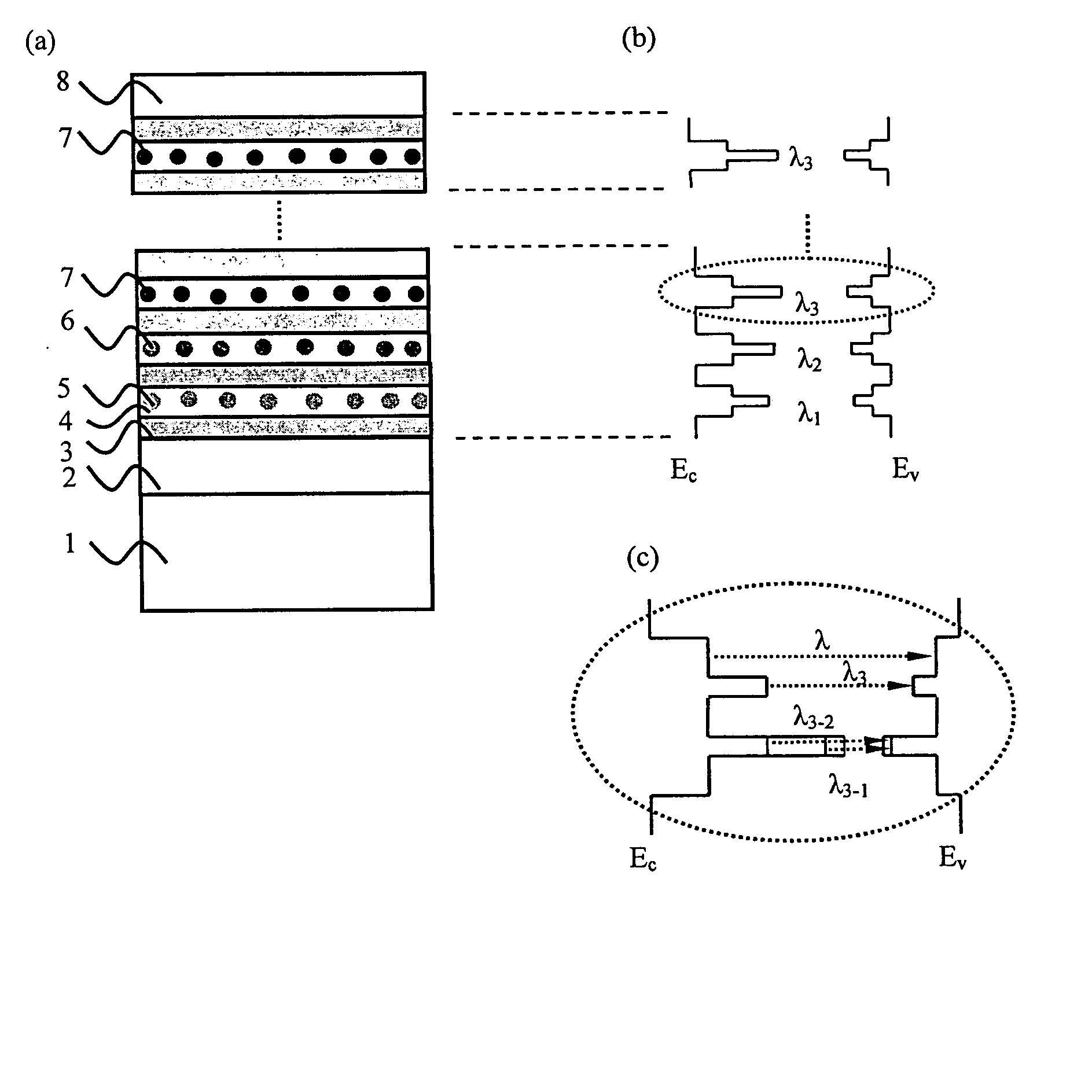
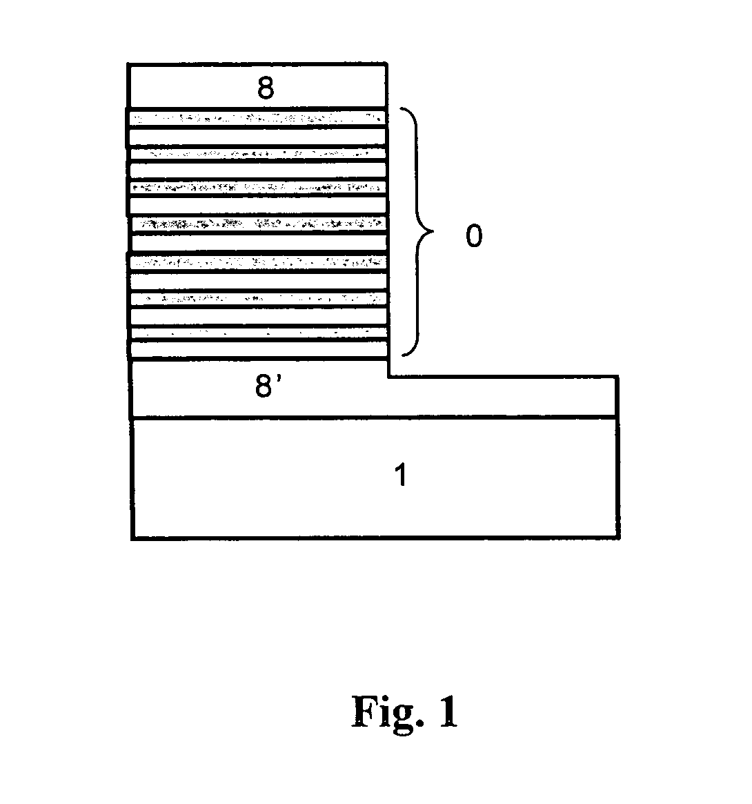
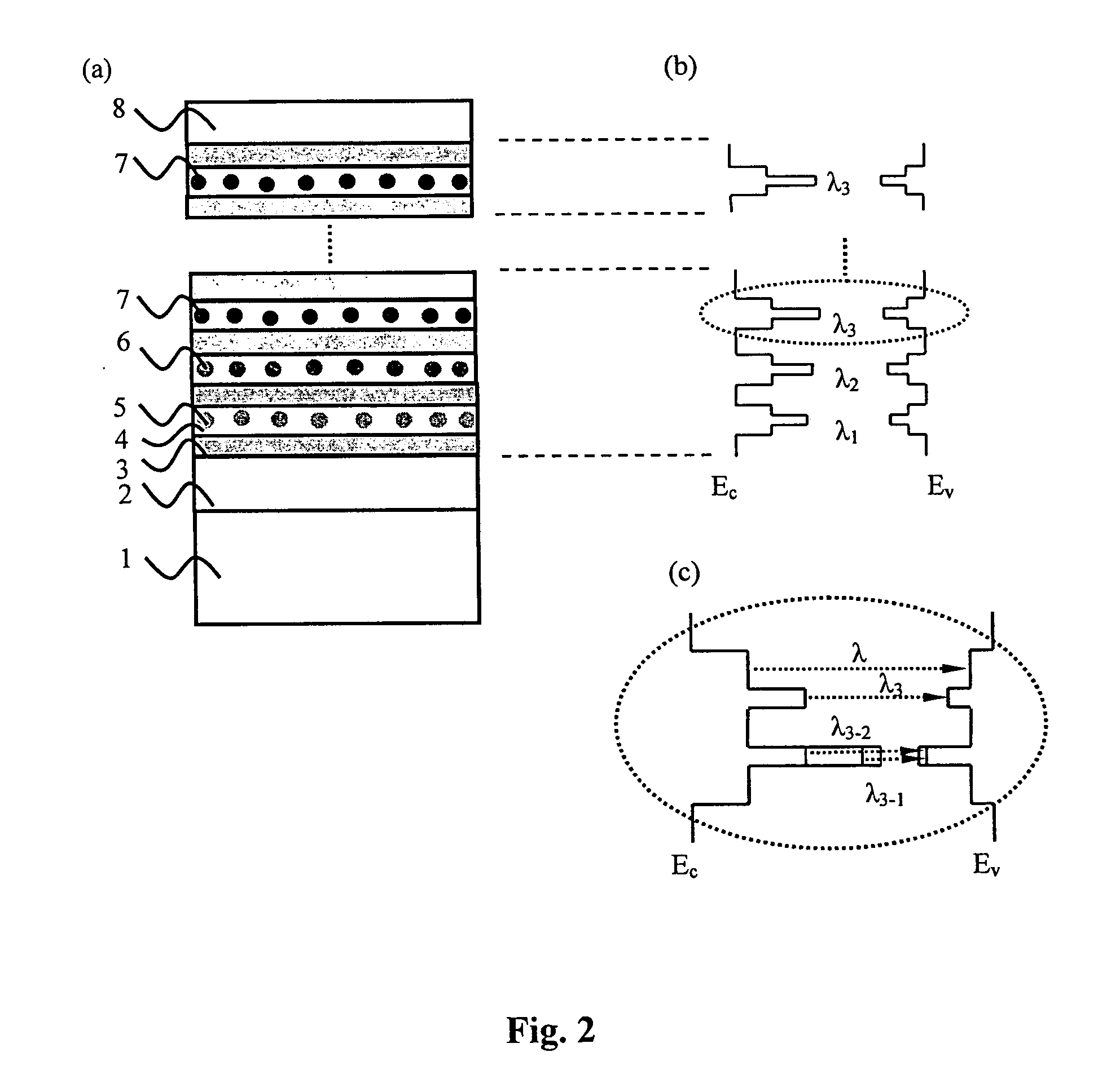
[0075] As to growth of nanoparticles in MQWs active layer structure effectively, which can reduce non-radioactive recombination rate resulted from dislocation in current MQWs active layers of Group III nitride LEDs, the present invention provides a nanoparticle-containing MQWs structure with single wavelength as active layer, as shown in FIG. 5(a), to elevate emitting efficiency of LEDs. The process comprises steps of, firstly providing a substrate 1 and growing n (or p) type buffer layer 2 on substrate 1, thereafter growing barrier layer 3; then growing lower energy well layer 4 and growing a nanoparticle structure with single wavelength λ1 therein; further growing higher energy barrier layer 3 to complete the single layer quantum well containing nanoparticle structure as active layer. The emitting efficiency of LEDs can be elevated by repeatedly growing the above structure or adjusting growing parameters like tempera...

example 2

Dichroic-Wavelengths LED Using Nanoparticle-Containing Active Layer

[0077] It is known from the above that the emitting wavelengths of the nanoparticles can be obtained by controlling the elemental composition and geometric size thereof. Accordingly, nanoparticles with different elemental composition and geometric size can be grown on different layers inside the MQWs active layer structure, and light emitting diodes with various wavelengths are manufactured. With the emitting properties of the nanoparticle-containing MQWs active layer, it is advantageous to develop white light emitting diodes with practical uses in the lighting applications.

[0078] Therefore, various designs of nanoparticle-containing MQWs structure as active layer are provided in the present invention to hybridize white light. Firstly, a design called “Dichroic wavelengths LED using nanoparticle-containing active layer” is described. Complementary colors generating white light under irradiation of D65 standard ligh...

example 3

RGB LED Using Nanoparticle-Containing Active Layer

[0081] As white light hybridized through combination of the primary colors is of high color rendering, thus is advantageous, nanoparticle-containing MQWs structure with the primary color wavelengths as active layer is provided in the present invention, as shown in FIG. 11(a), to hybridize white light. The related energy bands are shown in FIG. 11(b). First (λ1), second (λ2) and third (λ3) wavelengths denote individual color of the primary colors. Said nanoparticle-containing MQWs structure with the primary color wavelengths as active layer is produced by growing nanoparticles with first emitting wavelength (λ1) in first well layer 4, growing nanoparticles with second emitting wavelength (λ2) in second well layer 4, and growing nanoparticles with third emitting wavelength (λ3) in third well layer 4, then repeatedly growing a plurality of nanoparticle-containing MQWs structures with wavelengths 1, 2 and λ3 in this order to hybridize w...


PUM


Abstract

A structure of multi-wavelength light emitting device comprises multi-stacked active layer structure. Each stacked layer comprises lower energy bandgap well 4 and higher energy bandgap barrier layer 3 wherein at least one stacked layer in the device contains nanoparticles. As a result, the emitting wavelengths of the multi-stacked active layer structure consist parts (or all) of the emitting wavelengths come from the stack layers containing nanoparticles, and parts (or all) of the emitting wavelengths come from the stack layers not containing nanoparticles. In another embodiment, parts (or all) of the emitting wavelengths of the multi-stacked active layer structure can be also used to trigger one or more phosphorescences from the phosphors, thus the emitting wavelengths of such a phosphors converted light emitting device may come partially from the multi-stacked active layer itself and partially (or all) from the phosphors.

Description

FIELD OF THE INVENTION [0001] The present relates to a novel structure of light emitting device, particularly to a structure consisting of nanoparticles embedded in active layer, and manufacturing process thereof. The structure is useful in the production of any optoelectronic semiconductor devices with hetero junctions. DESCRIPTION OF THE RELATED PRIOR ART [0002] According to the research about light sources in energy saving and environmental protection, light emitting diode has become particularly attractive due to its low power consumption. [0003] In view of the current white light emitting diodes and manufacturing method, there are three main categories comprising: (1) complementary dichroism wherein white light is hybridized by triggering yellow phosphor particles with blue light form light emitting diode; (2) UV-LED pumping phosphors wherein white light is hybridized by triggering RGB phosphor particles with UV light from light emitting diode; and (3) three primary color light...

Claims


Application Information

Patent Timeline
Patent Type & Authority Applications(United States)
IPC IPC(8): H01J1/62H01L33/08H01L33/18H01L33/50
CPCB82Y20/00C09K11/0883C09K11/584C09K11/613C09K11/642C09K11/7731C09K11/7734C09K11/7774C09K11/7789C09K11/7791C09K11/7792C09K11/883H01L33/08H01L33/18H01L33/50C09K11/08
Inventor CHEN, WEI-KUOKE, WEN-CHENG
Owner NAT CHIAO TUNG UNIV
Why Eureka
Try Eureka