Capacitive load driving circuit, electrostatic transducer, method of setting circuit constant, ultrasonic speaker, display device, and directional acoustic system

a technology of electrostatic transducer and driving circuit, which is applied in the direction of piezoelectric/electrostrictive transducer, transducer type, instrument, etc., can solve the problems of large power loss than in the case of resistive load generation, poor reproduction sound quality, and very narrow frequency band of the circuit, so as to enhance the low frequency sound range and improve the sound presence. , the effect of low loss

Inactive Publication Date: 2007-05-31
SEIKO EPSON CORP
View PDF6 Cites 46 Cited by
  • Summary
  • Abstract
  • Description
  • Claims
  • Application Information

AI Technical Summary

Benefits of technology

[0079] Accordingly, the ultrasonic speaker that can drive with the low loss and has the flat output frequency characteristic may be used in the directional acoustic system. The ultrasonic speaker may be driven by the class-D power amplifier. For this reason, the acoustic signal of the medium and high frequency sound ranges having sufficient sound pressure and the broadband characteristic may be reproduced. In addition, since the acoustic of the low frequency sound range is directly outputted from the low frequency sound reproducing speaker provided in the acoustic system, the low frequency sound range is enhanced. Accordingly, it is possible to produce sound field environments having improved sound presence.

Problems solved by technology

However, the piezoelectric transducer may obtain a high sound pressure by using a fine resonance characteristic of elements, but the frequency band thereof is very narrow.
For this reason, the ultrasonic speaker using the piezoelectric transducer have problems in which the reproducible frequency band is narrow, and a reproduced sound quality is poor as compared to a loudspeaker.
However, when the electrostatic transducer is driven by an analog amplifier, there have been problems as follows.
Therefore, the power loss larger than that in the case of the resistive load is generated in the transistor.
As described above, if the load resistance RL value connecting to the LC low-pass filter is too low, the frequency characteristic becomes too dull, thereby gain degradation in the driving frequency band becomes large.
Therefore, it may be impossible to obtain the flat frequency characteristic, and the operation may be unstable in the worst case.
More particularly, when the electrostatic transducer is used as the ultrasonic speaker, if the flat frequency characteristic is not obtained, the reproduced sound quality becomes poor.
If an external resistance having a proper value is connected to the electrostatic transducer, it can obtain the flat frequency characteristic, but in exchange therefor the large power loss is generated due to the resistance.
Further, since the negative feedback is performed from the back of the second-order LC low-pass filter, a phase rotational amount of the negative feedback signal may be restricted within 180 degrees.
For this reason, since a damping slope of the low-pass filter increases in the switching frequency band of the power switching circuit (the output stage or the like of the class-D power amplifier), the switching carrier components are sufficiently removed in the power switching circuit output, and thus the output noise becomes small.

Method used


Image

  • Capacitive load driving circuit, electrostatic transducer, method of setting circuit constant, ultrasonic speaker, display device, and directional acoustic system
  • Capacitive load driving circuit, electrostatic transducer, method of setting circuit constant, ultrasonic speaker, display device, and directional acoustic system
  • Capacitive load driving circuit, electrostatic transducer, method of setting circuit constant, ultrasonic speaker, display device, and directional acoustic system

Examples


first embodiment

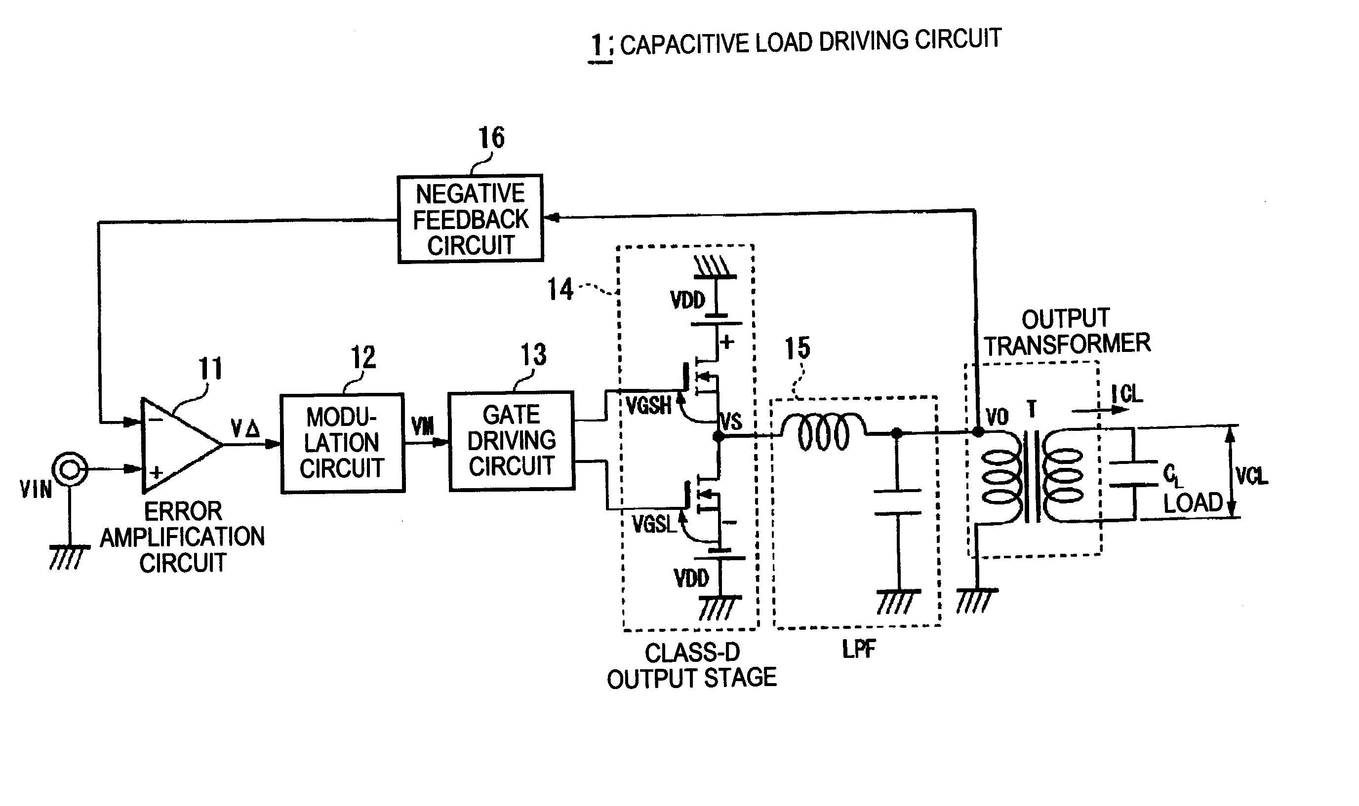
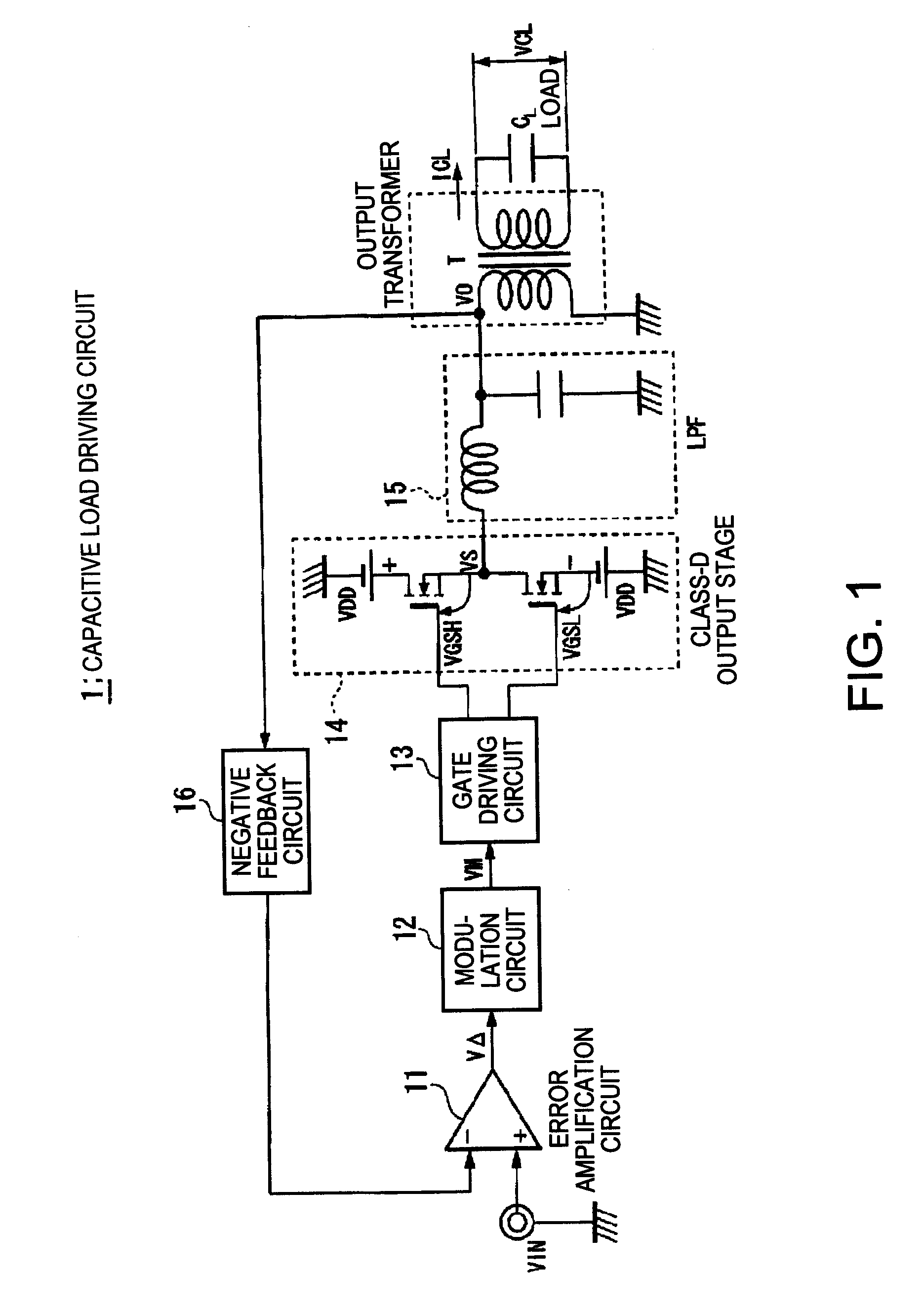
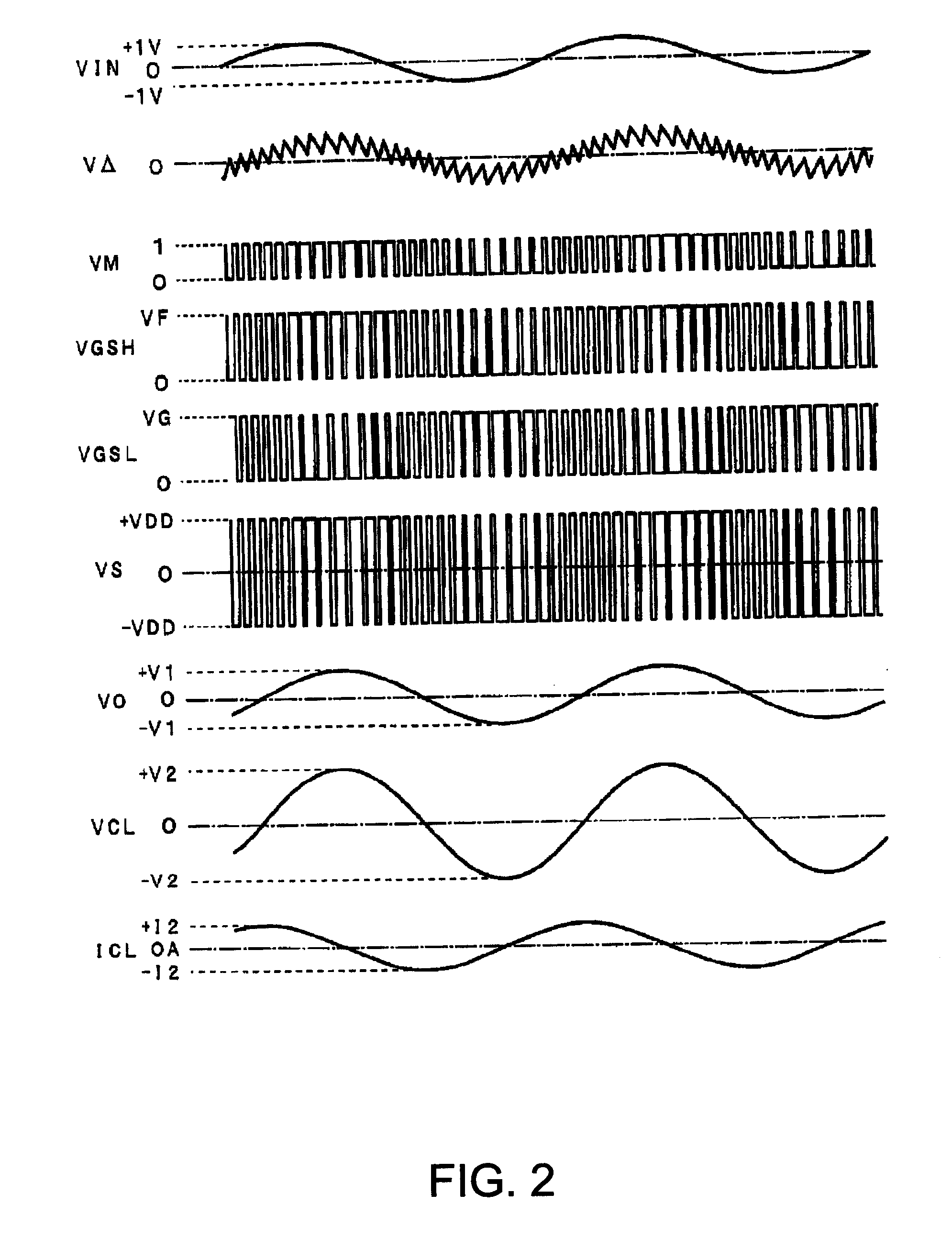
[0106]FIG. 1 is a view showing a structure example of a capacitive load driving circuit according to an embodiment of the present invention. In addition, FIG. 2 is a view showing an example of an operation waveform of each part.

[0107] As shown in FIG. 1, the capacitive load driving circuit 1 according to the embodiment of the present invention includes an error amplification circuit 11, a modulation circuit 12, a gate driving circuit 13, class-D output stage 14, LC low-pass filter (LPF) 15, a negative feedback circuit 16, an output transformer T, and a load capacitance CL as a basic structure element.

[0108] The error amplification circuit 11 amplifies a difference between a signal VIN inputted from an outside and a signal from the negative feedback circuit (described later). The external input signal VIN is inputted to a non inverting input terminal (+) of the error amplification circuit 11, and a feedback signal from the negative feedback circuit 16 is inputted to an inverting in...

second embodiment

[0169] The second exemplary embodiment of the present invention is explained below.

[0170]FIG. 13 is a view showing a circuit structure example of a full-bridge driven in a balance output using a pair of gate driving circuits, class-D output stages, and LC filters.

[0171] PWM signals supplied to the gate driving circuit A 131 and the gate driving circuit B 132 from the PWM modulation circuit 12A are inverted in phase with each other. Therefore, the class-D output stage A141 and the class-D output stage B142 perform a switching operation in an inverted phase state with each other. The output that is obtained from the LPFA 151 and LPFB 152 of the LC low-pass filter is a balance output.

[0172] A phase compensation circuit A 171 and a phase compensation circuit B 172 perform phase lead compensations with respect to each output of the LPFA 151 and LPFB 152. At this time, a voltage is damped to an input level of the differential amplifier 161. Then, it is configured such that a voltage di...

third embodiment

[0175] The third exemplary embodiment of the present invention is explained below.

[0176] Referring to FIG. 14, the balance output from the LPFA 151 and the LPFB 152 is amplified by the differential amplifier 161, and then converted into digital values in an A / D converter 162. Thereafter, error detection between a feedback signal and an input signal and PWM modulation are performed. That is, FIG. 14 shows the configuration where all the successive processes are performed by digital processing. The error calculating unit 11B detects an error between the feedback signal and the input signal, and the control unit 11C controls the ratio of PWM modulation such that an error between input and output (input signal IN and FB signal) is zero. The PWM modulation circuit 12A modulates the output from the control unit 11C using PWM modulation method.

[0177] In addition, the error calculating unit 11B, the control unit 11C, and the PWM modulation circuit 12A are configured as a processing unit s...


PUM


Abstract

A capacitive load driving circuit includes an error amplification circuit that amplifies a difference between an external input signal provided to one input terminal and a negative feedback signal provided from the following negative feed back circuit to the other input terminal; a modulation circuit that pulse-modulates the signal outputted from the error amplification circuit; a power switching circuit that switches between a power supply voltage and a ground potential or between a positive power supply voltage and a negative power supply voltage; a gate driving circuit that generates a gate driving signal for switching-controlling a switching element configuring the power switching circuit, from a modulated signal outputted from the modulation circuit; a low-pass filter that is connected to an output side of the power switching circuit and removes switching carrier components included in an output signal of the power switching circuit; an output transformer that boosts an output signal of the low-pass filter and has a primary winding connected to an output terminal of the low-pass filter; a capacitive load that is connected in parallel with a secondary winding of the output transformer; and a negative feedback circuit that performs a negative feedback from the output terminal of the low-pass filter to an input side of the error amplification circuit.

Description

CROSS-REFERENCE TO RELATED APPLICATION [0001] This application claims priority from Japanese Patent Application Nos. 2005-343307 and 2006-281683, filed in the Japanese Patent Office on Nov. 29, 2005 and Oct. 16, 2006, respectively, the entire disclosures of which are hereby incorporated by reference in their entireties. BACKGROUND [0002] 1. Technical Field [0003] The invention relates to a capacitive load driving circuit using class-D (digital) power amplifier, an electrostatic transducer, a method of setting a circuit constant, an ultrasonic speaker, a display device, and a directional acoustic system, and more particularly, to a circuit configuration of class-D power amplifier that is suitable for driving the ultrasonic speaker for reproducing a sound having fine directivity by outputting a modulation wave, of which a carrier wave in an ultrasonic frequency band is modulated by an acoustic signal in an audible frequency band, from the electrostatic transducer serving as a capaciti...

Claims


Application Information

Patent Timeline
Patent Type & Authority Applications(United States)
IPC IPC(8): G06F1/00
CPCG03B21/14H03F1/34H03F3/2171H03F3/2173H03F2200/03H03F2200/345H03F2200/351H03F2200/45H03F2200/541H04R19/02H04R2217/03
Inventor MIYAZAKI, SHINICHI
Owner SEIKO EPSON CORP
Why Eureka
Try Eureka