Group iii nitride crystal and manufacturing method thereof

a technology of nitride crystals and manufacturing methods, applied in the direction of crystal growth process, polycrystalline material growth, under a protective fluid, etc., can solve the problem of difficult to reduce the dislocation density, and achieve the effect of reducing the dislocation density and allowing the penetration of thread dislocations

Active Publication Date: 2007-06-07
SUMITOMO CHEM CO LTD +1
View PDF21 Cites 24 Cited by
  • Summary
  • Abstract
  • Description
  • Claims
  • Application Information

AI Technical Summary

Benefits of technology

[0042] According to the present invention, a group III nitride crystal containing therein an alkali metal is manufactured by consecutively causing crystal growth processes of the first group III nitride crystal that deflects the threading dislocations in the direction different from the direction of crystal growth from the base body, and the second group III nitride crysta

Problems solved by technology

In the case of growing a group III nitride crystal on a base body by reacting a melt mixture of alkali metal and group III metal with a group V source material including nitrogen, on the other hand, there arises a problem, when the base body con

Method used


Image

  • Group iii nitride crystal and manufacturing method thereof
  • Group iii nitride crystal and manufacturing method thereof
  • Group iii nitride crystal and manufacturing method thereof

Examples


embodiment 1

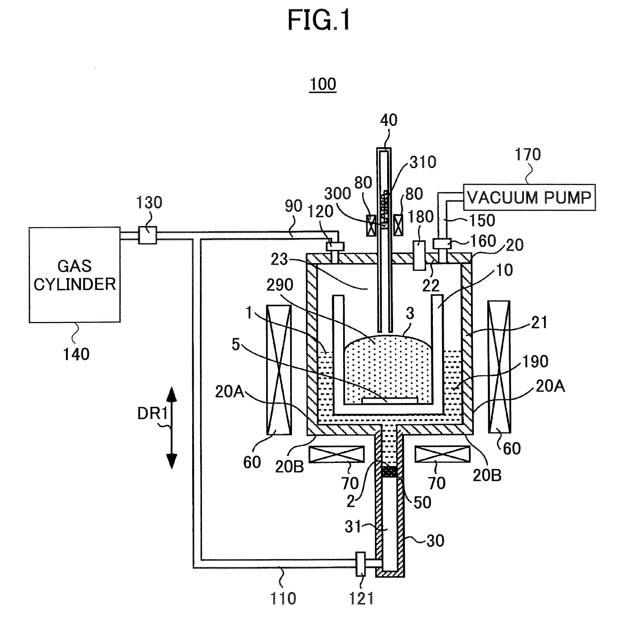
[0075]FIG. 1 is a schematic cross-sectional diagram showing the construction of a crystal growth apparatus according to Embodiment 1 of the present invention. Referring to FIG. 1, the crystal growth apparatus 100 of Embodiment 1 comprises a reaction vessel 10, an outer reaction vessel 20, conduits 30 and 40, a stopper / inlet plug 50, heating units 60, 70 and 80, gas supply lines 90 and 110, valves 120, 121 and 160, a pressure regulator 130, a gas cylinder 140, an evacuation line 150, a vacuum pump 170, a pressure sensor 180, and a metal melt 190.

[0076] The reaction vessel 10 has a generally cylindrical form and is formed of boron nitride (BN). The outer reaction vessel 20 is disposed around the reaction vessel 10 with a predetermined separation from the reaction vessel 10. Further, the outer reaction vessel 20 is formed of a main part 21 and a lid 22. Each of the main part 21 and the lid 22 is formed of SUS 316L stainless steel, wherein a metal seal ring is provided between the main...

embodiment 2

[0193]FIG. 15 is a schematic cross-sectional diagram showing a crystal growth apparatus according to Embodiment 2 of the present invention. Referring to FIG. 15, a crystal growth apparatus 100A has a construction generally identical with the construction of the crystal growth apparatus 100, except that a bellows 200, support unit 210, an up / down mechanism 220, a vibration application unit 230, and a vibration detection unit 240 are added to the crystal growth apparatus 100 shown in FIG. 1.

[0194] The bellows 200 is connected to the outer reaction vessel 20 at a location above the reaction vessel 10 in terms of the gravitational direction DR1. The support unit 210 comprises a cylindrical member and a part thereof is inserted into the space 23 inside the outer reaction vessel 20 via the bellows 200. The up / down mechanism 220 is mounted upon the support unit 210 at the location above the bellows 200.

[0195] The bellows 200 holds the support unit 210 and disconnects the interior of the ...

embodiment 3

[0250]FIG. 23 is a schematic cross-sectional diagram showing a crystal growth apparatus according to Embodiment 3 of the present invention. Referring to FIG. 23, a crystal growth apparatus 100B of Embodiment 3 has a construction generally identical with the construction of the crystal growth apparatus 100 shown in FIG. 1, except that the conduit 40 and the heating unit 80 are removed.

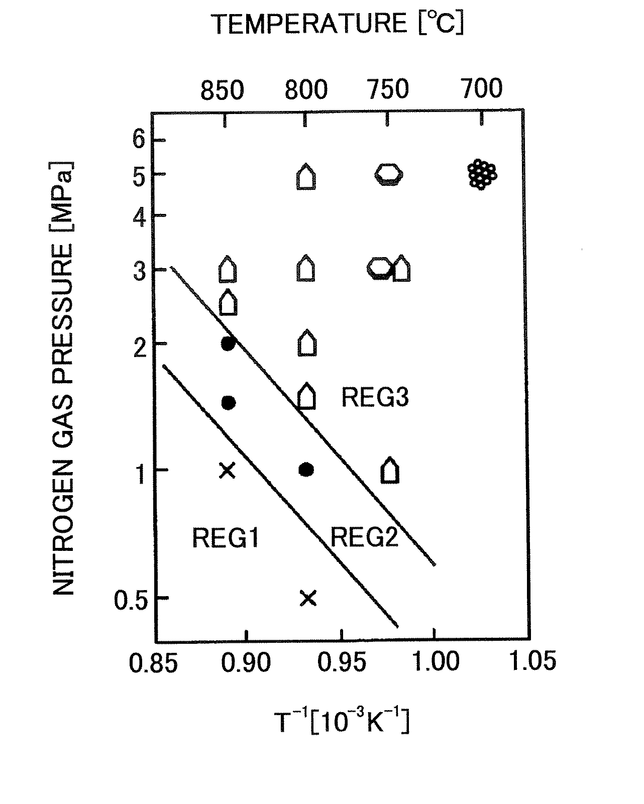
[0251] With the crystal growth apparatus 100B, the reaction vessel 10 holds a melt mixture 320 in place of the melt mixture 290. The melt mixture 320 comprises a melt mixture of metal Na and metal Ga.

[0252]FIG. 24 is a timing chart showing the temperature of the reaction vessel 10 and the outer reaction vessel 20 and a Li concentration in the melt mixture 320. Referring to FIG. 24, the temperatures of the reaction vessel 10 and the outer reaction vessel 20 are elevated in the crystal growth apparatus 100B along the curve k2 and are held at 800° C. similarly to the crystal growth apparatus 100.

[0253] ...


PUM


Abstract

A group III nitride crystal containing therein an alkali metal element comprises a base body, a first group III nitride crystal formed such that at least a part thereof makes a contact with the base body, the first group III nitride crystal deflecting threading dislocations in a direction different from a direction of crystal growth from the base body and a second nitride crystal formed adjacent to the first group III nitride crystal, the second nitride crystal having a crystal growth surface generally perpendicular to the direction of the crystal growth.

Description

TECHNICAL FIELD [0001] The present invention relates to group III nitride crystals and manufacturing method thereof. [0002] These days, most of the InGaAlN (a group III nitride semiconductor) devices used for ultraviolet, purple, blue and green optical sources are formed on a substrate of sapphire or silicon carbide (SiC) by conducting thereon an MOCVD process (metal-organic chemical vapor deposition process) or MBE process (molecular beam epitaxy process). [0003] In the case sapphire or silicon carbide is used for the substrate, however, there are formed a large number of crystal defects in the group III nitride semiconductor layers grown thereon in view of the fact that there exists a large difference in the thermal expansion coefficient and lattice constant between the substrate and the group III nitride semiconductor layers. Such crystal defects invite deterioration of device performance and are related directly to the drawbacks such as short lifetime, large operational power, a...

Claims


Application Information

Patent Timeline
IPC IPC(8): H01L21/00H01L29/22
CPCC30B9/00C30B29/403H01L21/0242H01L21/02458H01L21/0254H01L21/02573H01L21/02595H01L21/02625H01L21/02639H01L21/02647
Inventor IWATA, HIROKAZUSARAYAMA, SEIJIFUSE, AKIHIRO
Owner SUMITOMO CHEM CO LTD
Why Eureka
Try Eureka