Package for high power density devices

a high-power density, package technology, applied in the direction of semiconductor devices, semiconductor/solid-state device details, electrical apparatus, etc., can solve the problems of power loss and corresponding heating of semiconductor dies beyond the specified limits, package inductivity is also an important limiting factor for switching high curren

Active Publication Date: 2007-06-21
INFINEON TECH AMERICAS CORP
View PDF8 Cites 119 Cited by
  • Summary
  • Abstract
  • Description
  • Claims
  • Application Information

AI Technical Summary

Benefits of technology

[0018] In accordance with the invention a novel high current package is formed in which a depression formed in the top copper layer forms a “case” to receive a thinned semiconductor die such as a MOSFET or IGBT or the like. The drain contact (drain and collector electrodes are interchangably used herein) is soldered to the surface of the depression and the top surface of the die is approximately c

Problems solved by technology

The power and current carrying capabilities of power switches such as MOSFETs and IGBTs are commonly limited by their package.
Thus, the package introduces thermal and electrical resistance that can cause power loss and corresponding heating of the semiconductor die beyond its specified limits.
Beside the thermal issues, package inductivity is also an important limiting factor for switching high currents.
Parasitic package inductance causes inductive over-voltage that can destroy the die.
A major problem of large metal contacts or copper straps is the stress on the die due to the higher thermal expansion coefficient of metal compared to that of the die, such as a silicon based die.
This may be acceptable in relatively moderate power applications as in consumer electronics but it creates a severe reliability issue for heavy duty applications in a harsh environment like those of automotive electronics.
The stress effect in such extreme applications can cause major damage to the sensitive top metal layers of the die due to the active layers underneath.
Besides the introduced stress on the die, large metal contacts such as those used in a copper strap device or in the DirectFET device can metal, can have another disadvantage on the long term behavior of the package.
Thus, the solder joint between the die and the metal contact tends to deteriorate rapidly if major temperature changes and cycling are applied.
This failure mechanism is also driven by the thermal mismatch and the different thermal expansion of the metal contact vs. the die material.
This results in micro cracks and even de-lamination of the contact, causing an increase of thermal and electrical resistance within the solder joint.
Consequently, the package performance will be impacted.
However, an adhesive or glue layer has limited current carrying capability and a higher thermal resistance as comp

Method used


Image

  • Package for high power density devices
  • Package for high power density devices
  • Package for high power density devices

Examples


Embodiment Construction

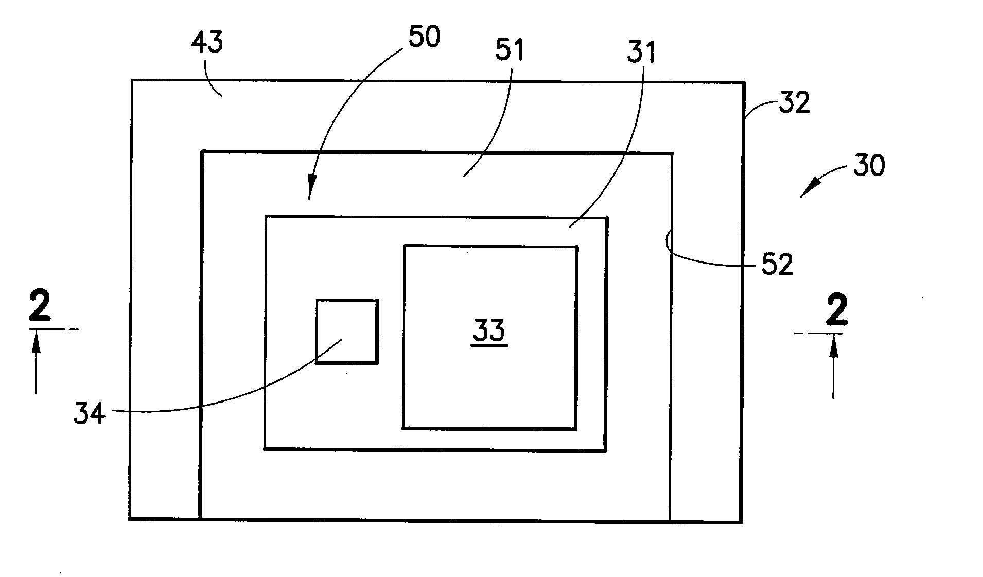
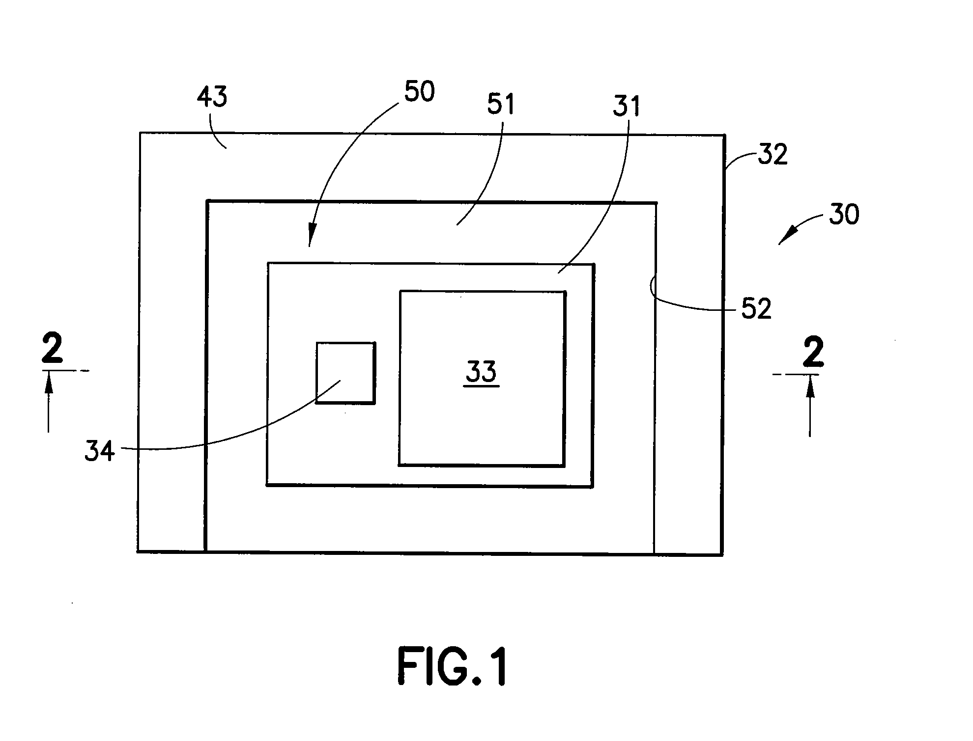
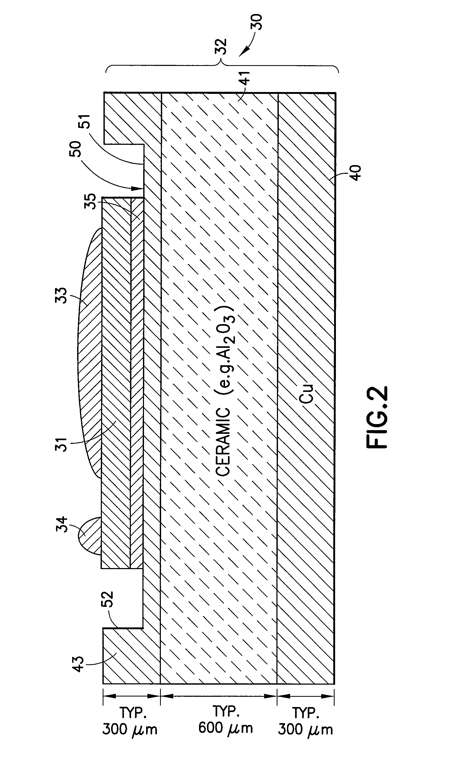
[0074]FIGS. 1, 2 and 3 show a first embodiment of the semiconductor device 30 of the invention. The semiconductor device 30 comprises a semiconductor die 31 and a housing 32.

[0075] Semiconductor die 31 may be a silicon based vertical conduction power MOSFET having, on one surface, a source electrode which receives a solder bump 33, a gate electrode which receives a solder bump 34 and, on its opposite surface, a drain electrode which receives solder preform 35. It should be noted that solderable metal pads can be used in place of the solder bumps and solder paste can be used in place of the solder preform. While die 31 is shown as a silicon die, it may be of any type of semiconductor material including Gallium Nitride based devices, silicon carbide devices and the like. Further, while die 31 is described as a power MOSFET, it can be any type of semiconductor device, including a bipolar transistor die, an IGBT die, a break over device die, a diode die and the like. The term MOSgated ...


PUM


Abstract

A semiconductor device package is formed of DBC in which thinned MOSgated and/or diode die are soldered to the bottom of an etched depression in the upper conductive layer. A via in the insulation layer of the DBC is filled with a conductive material to form a resistive shunt. Plural packages may be formed in a DBC card and may be separated individually or in clusters. The individual packages are mounted in various arrays on a support DBC board and heat sink. Integrated circuits may be mounted on the assembly and connected to the die for control of the die conduction.

Description

RELATED APPLICATIONS [0001] The present application is based on and claims benefit of U.S. Provisional Application No. 60 / 753,353, filed Dec. 21, 2005, entitled BOND-WIRELESS HIGH POWER DENSITY MODULE WITH INTEGRATED SMARTNESS (IR-3174 Prov); U.S. Provisional Application No. 60 / 756,984, filed Jan. 6, 2006, entitled BOND-WIRELESS POWER PACKAGE WITH INTEGRATED CURRENT SENSOR, ESPECIALLY SHORT CIRCUIT PROTECTION (IR-3175 Prov); and Provisional Application No. 60 / 761,722, filed Jan. 24, 2006, entitled STRESS-REDUCED BOND-WIRELESS PACKAGE FOR HIGH POWER DENSITY DEVICES (IR-3177 Prov), to all of which a claim of priority is hereby made and the disclosure of which is incorporated by reference.FIELD OF THE INVENTION [0002] This invention relates to semiconductor device packages and to processes for their manufacture. BACKGROUND OF THE INVENTION [0003] The power and current carrying capabilities of power switches such as MOSFETs and IGBTs are commonly limited by their package. Thus, the pack...

Claims


Application Information

Patent Timeline
IPC IPC(8): H01L23/48
CPCH01L23/13H01L2924/1305H01L23/49838H01L24/83H01L24/97H01L25/072H01L25/16H01L2224/0401H01L2224/0603H01L2224/1403H01L2224/16H01L2224/48091H01L2224/73153H01L2224/73265H01L2224/83101H01L2224/83801H01L2224/92247H01L2224/97H01L2924/01013H01L2924/01025H01L2924/01029H01L2924/01047H01L2924/01077H01L2924/01078H01L2924/01082H01L2924/01327H01L2924/13055H01L2924/13091H01L2924/14H01L2924/15787H01L2924/19041H01L2924/19043H01L2924/30107H01L2924/3025H01L23/15H01L2924/1306H01L2224/32503H01L28/20H01L23/481H01L23/36H01L2224/291H01L24/48H01L2924/01005H01L2924/01006H01L2924/01033H01L2924/01068H01L2924/014H01L23/367H01L23/552H01L2224/32145H01L2224/48145H01L23/62H01L2224/83139H01L2924/10253H01L2224/26175H01L2924/00014H01L2924/05432H01L2924/00H01L2924/3512H01L2924/15747H01L2924/181H01L2224/14H01L2224/48227H01L2224/45099H01L2224/45015H01L2924/207H01L2924/00012H01L23/04
Inventor HAUENSTEIN, HENNING M.
Owner INFINEON TECH AMERICAS CORP
Why Eureka
Try Eureka