Semiconductor leakage current detector and leakage current measurement method, semiconductor leakage current detector with voltage trimming function and reference voltage trimming method, and semiconductor intergrated circuit thereof

a leakage current detector and leakage current measurement technology, applied in pulse manipulation, pulse technique, instruments, etc., can solve the problems of increasing the testing cost, affecting requiring expensive test equipment, so as to improve the accuracy of leakage current determination, shorten the trimming time, and increase the search speed

Active Publication Date: 2007-06-28
III HLDG 12 LLC
View PDF11 Cites 86 Cited by
  • Summary
  • Abstract
  • Description
  • Claims
  • Application Information

AI Technical Summary

Benefits of technology

[0094] This configuration allows removing the influences of the input offset of the comparator, increasing the speed of searching a second trimming intermediate value, and shortening the trimming time.
[0095] As described in the above, the semiconductor leakage current detector of the present invention can make a highly accurate determination of the leakage current at high speed using a simple measurement algorithm by canceling errors resulted from the system of measurement such as variations of integral capacitors and input offset voltage of the comparator, and removing noises superimposed on the current to be measured through the integral operation.

Problems solved by technology

In order to measure a few thousands of bit lines constituting a memory array, testing time of around a few tens of seconds is thus required causing a huge impact on the testing cost.
However, since such parallel measurement requires a test resource independent for each device of the test equipment, expensive test equipment is required.
Furthermore, with regard to the testing cost, the internal reference voltage source, that controls the accuracy of internal voltage in the device, requires a process (trimming) of adjusting each device at a reference value, contributing to the increase of the testing cost.
As described above, since the measurement of the bit line leakage current and the trimming of the reference voltage source are required for non-volatile memories manufactured through fine processing to maintain high reliability, there is a problem that tests for these non-volatile memories cause increases of the testing time, cost of the test equipment and costs for testing including throughput.

Method used


Image

  • Semiconductor leakage current detector and leakage current measurement method, semiconductor leakage current detector with voltage trimming function and reference voltage trimming method, and semiconductor intergrated circuit thereof
  • Semiconductor leakage current detector and leakage current measurement method, semiconductor leakage current detector with voltage trimming function and reference voltage trimming method, and semiconductor intergrated circuit thereof
  • Semiconductor leakage current detector and leakage current measurement method, semiconductor leakage current detector with voltage trimming function and reference voltage trimming method, and semiconductor intergrated circuit thereof

Examples


first embodiment

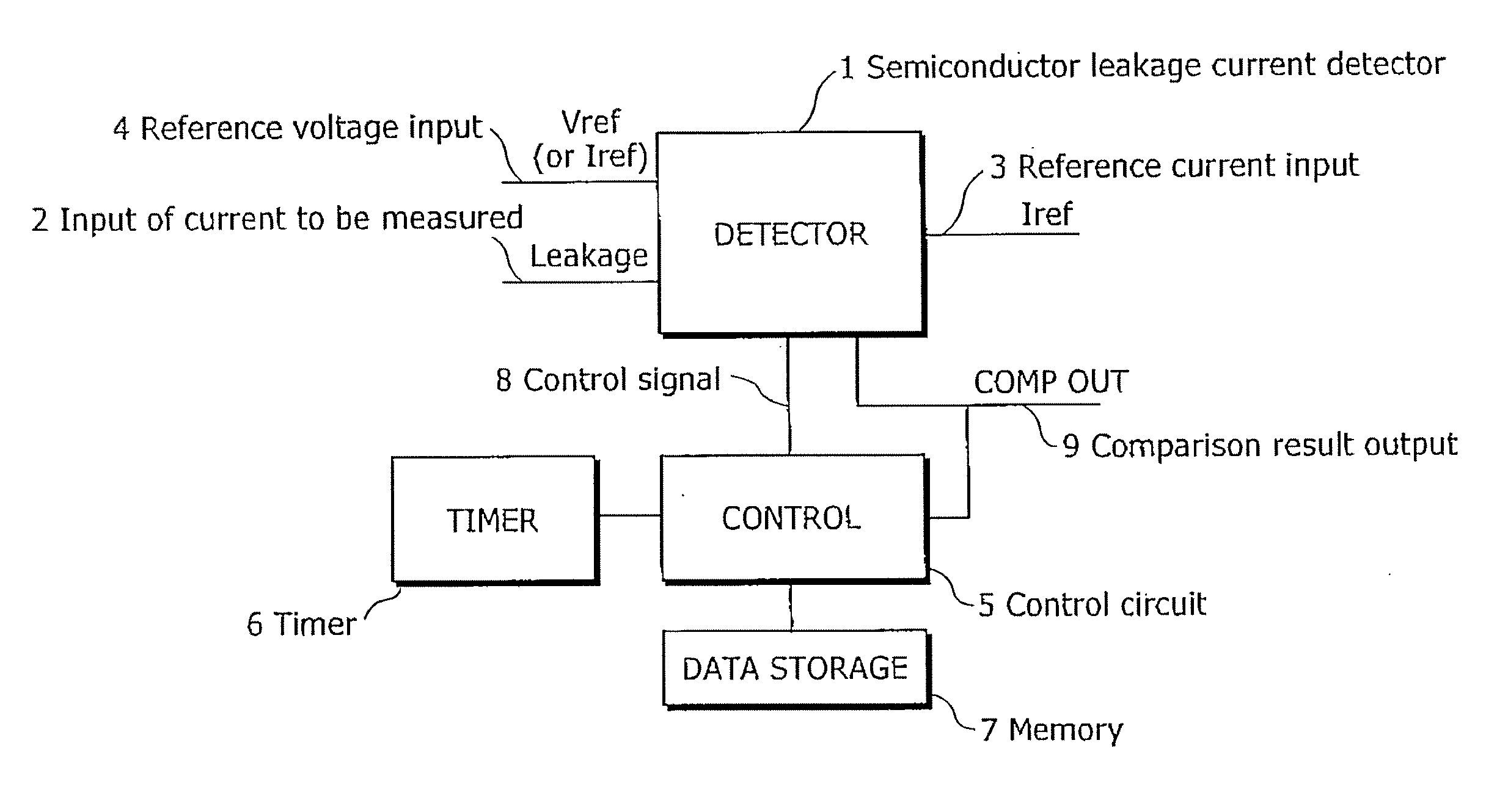
[0127]FIG. 3 is a schematic circuit diagram of a semiconductor leakage current detector according to the first embodiment of the present invention. In FIG. 3, a reference voltage Vref is supplied to a reference-side input 31 of a comparator 30 from a reference voltage circuit 43, and an integral voltage Vint is supplied to an integral capacitor-side input 32 to which the integral capacitor 34 is connected. A discharge transistor 35 is connected in parallel to the integral capacitor 34 (Cd), and discharges a charge to a ground level. A measured circuit 44, which is a circuit to be measured, Is made up of bit lines of a memory and the like, and supplies a current to be measured 46 (Ileak) to the integral capacitor 34 through a second analog switch 40. Furthermore, the reference current circuit 45 supplies a reference current 47 (Iref) to the integral capacitor 34 via a first analog switch 39. A stray capacitor 38 (Cs) is connected to a current path of the measured circuit 44, and a co...

second embodiment

[0146]FIG. 4 is a schematic circuit diagram of a semiconductor leakage current detector with a greater range of application in which the compensation capacitor is varied, in addition to the configuration described in the first embodiment. In FIG. 4, the compensation capacitor is made up of a metal option unit 400 and a control option unit 401, as a compensation capacitor circuit. The metal option unit 400 sets a gate voltage of the transistor which is connected to the capacitor in series, based on the potential of the metal layer connected to the gate, and sets a fixed value portion of the compensation capacitor. Also, the metal option unit 400 is connectable to a wiring layer during a manufacturing process (mask option, etc.) in order to determine the capacitance value of the compensation capacitor. The control option unit 401 selectively sets the potential of the gate of the transistor which is connected to the capacitor in series, and sets the variable portion of the compensation...

fourth embodiment

[0165] The fourth embodiment describes an example of a semiconductor leakage current detector which is reduced in area by using an accumulation-type MOS capacitor for the integral capacitor according to the first embodiment. In the first embodiment, the voltage level of the integral capacitor ranges from several tens mV to several hundreds mV, and is in a range less than a threshold value of the MOS capacitor, in order to increase the determination speed.

[0166] In such low voltage area, a substrate of a commonly-used depletion-type CMOS capacitor is in a depletion state, causing a problem that the capacitance value equivalent to a fraction of a capacitance of normal inverted region. In order to solve this problem, it is preferred to use a Pch accumulation-type MOS capacitor as an integral capacitor. FIG. 6 is an explanatory diagram of the Pch accumulation-type MOS capacitor. In FIG. 6, the accumulation capacitor biases the Pch accumulation-type MOS capacitor placed under the gate o...


PUM


Abstract

A semiconductor leakage current detector of the present invention includes a first analog switch which causes a current to be measured to flow or to be cut off, a second analog switch which causes a reference current to flow or to be cut off, an integral capacitance element which is connected by the first analog switch and the second analog switch and is charged with the current to be measured or the reference current, a discharge unit which discharges the integral capacitor, and a comparison unit which compares the reference voltage with each of an integral voltage generated in the integral capacitor by a reference current after the discharge of the integral capacitor and an integral voltage generated in the integral capacitance element by the current to be measured after the discharge of the integral capacitor

Description

BACKGROUND OF THE INVENTION [0001] (1) Field of the Invention [0002] The present invention relates to a semiconductor leakage current detector and a leakage current measurement method for detecting a bit line leakage current of a flash memory and the like at high-speed and for executing on-chip trimming of a reference voltage, to a semiconductor leakage current detector with a voltage trimming function and a reference voltage trimming method, and to a semiconductor integrated circuit thereof. [0003] (2) Description of the Related Art [0004] In recent years, non-volatile memories such as a flash memory and an EEPROM are arranged as a large storage capacity memory array using fine memory cells in addition, as memory cells are finely processed, it has become essential that a non-volatile memory is equipped with a reference voltage source that supplies an accurate internal voltage necessary for rewrite and read-out operations. [0005] One of the problems the recent non-volatile memories ...

Claims


Application Information

Patent Timeline
Patent Type & Authority Applications(United States)
IPC IPC(8): G01R31/14
CPCG01R31/3008G11C29/02G11C29/025G11C29/028G11C29/50G11C2029/1204G11C2029/5006
Inventor TOMITA, YASUHIROKOMIYA, MANABUSUWA, HITOSHIMORI, TOSHIKI
Owner III HLDG 12 LLC
Why Eureka
Try Eureka