Optical modulation device, optical transmitter, and optical transmission equipment

Inactive Publication Date: 2007-06-28
HITACHI LTD
View PDF8 Cites 19 Cited by
  • Summary
  • Abstract
  • Description
  • Claims
  • Application Information

AI Technical Summary

Benefits of technology

[0025]Furthermore, if the optical modulation device is configured to allow the above-mentioned information to be inputted and outputted from/to the each optical transmission equipment or remote control console, there is the effect of capability of automatically or remotely monitoring a state of this optical modulator and controlling its operation.
[0026]This invention has an effect that solves the three problems described above in the optical modulation device, which is typified by the CSRZ modulation device, and enables the stabilization control of the bias-voltage using the same control algorithm and circuit (for example, minimization control circuit) regardless the clock amplitude. As a result, it becomes possible to realize an optical transmitter even in a range where the clock amplitude is 60-80% of V2π of the optical modulator to which the conventional control method cannot be applied. Moreover, this invention provides several effects: An allowable range of characteristic variation of the modulator and high-frequency parts and specification alteration is widened, procurement costs of parts are reduced, procurement of parts is made easier, design alteration in the future is facilitated, etc. Furthermore, since the clock amplitude can be made variable in a wider range, this invention provides an advantage of realizing an optical transmitter capable of changing its waveform and duty ratio.
[0027]In addition, since by performing the bias control that uses the control light being transmitted through an optical modulator in an opposite direction, the control light is hardly modulated with a high-frequency signal in this invention, the invention provides an effect that the bias point becomes resistant to a change of the modulation scheme of a modulated waveform and a variation in the waveform, such as the duty ratio of the waveform. Consequently, the control scheme and circuit of this invention can be used commonly in a plural

Problems solved by technology

Firstly, there is a problem that a range exists to which stabilization control cannot be applied depending on the clock amplitude.
In a frequency band exceeding 10 GHz that is normally used for optical communications, IC's and driver amplifiers capable of outputting such a high voltage will be expensive and difficult to obtain.
However, in the range of the clock amplitude of 80% to 60%, automatic control cannot be applied in the conventional scheme.
Even being out of this range, in the case of near this range (for example, a range of 90 to 50%), since the average optical power characteristic of FIG. 6C is almost flat, there is a problem that, even if the bias-voltage changes, a change in the average optical power is small; therefore, actually control precession becomes extremely poor, and it is not suitable to practical use.
Moreover, there is a problem that, when the clock amplitude is reduced to 40% or less, the degree of modulation degree falls and the optical output power from an optical transmitter decreases sharply.
Consequently, in the conventional example, the clock amplitude applied to the MZ modulator cannot be set up freely, which obstructs cost reduction and part procurement.
Secondly, there is a problem that an allowable margin for parts are small, which makes it difficult to manufacture an optical transmitter.
Regarding high-frequency signals over a few

Method used


Image

  • Optical modulation device, optical transmitter, and optical transmission equipment
  • Optical modulation device, optical transmitter, and optical transmission equipment
  • Optical modulation device, optical transmitter, and optical transmission equipment

Examples


first embodiment

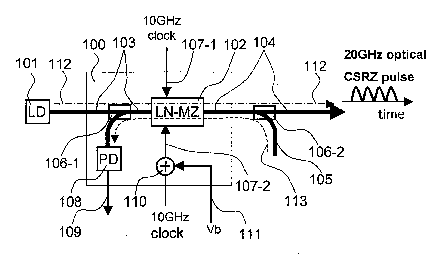
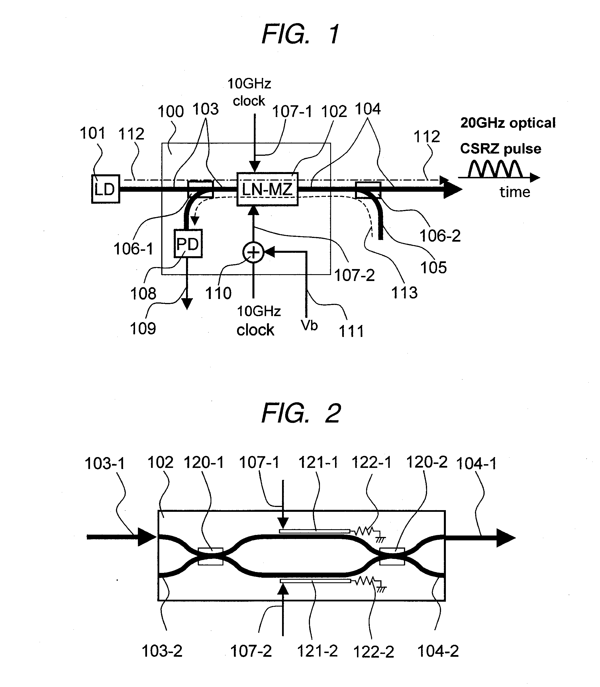
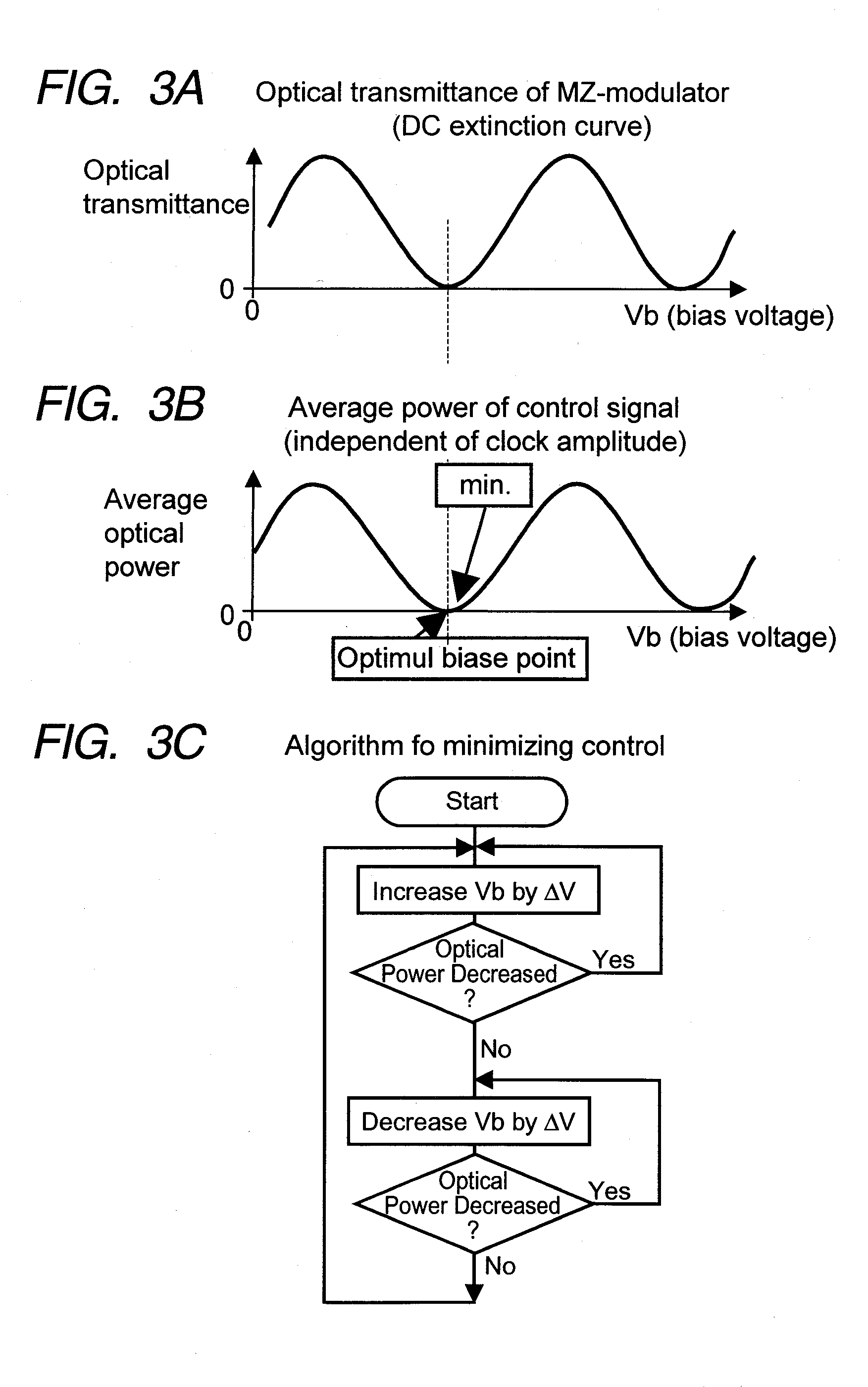
[0063]FIG. 1 is a block diagram showing a first embodiment of this invention, which is an example where an optical modulation device 100 of this invention is applied for formation of the CSRZ optical pulse. The laser beam outputted from the laser optical source 101 advances along the path 112 of the signal light in the figure, is inputted into the optical modulator 102 from the light input path 103-1, and outputted as the CSRZ optical pulse from the light output path 104. As the optical modulator 102, a general dual-drive LN-MZ modulator is used, and the sinusoidal wave clock signals of a frequency of 10 GHz whose phases are mutually reversed are applied to the two traveling-wave type input terminals 107-1, 107-2. A generation principle of the CSRZ optical pulse is the same as that of the conventional example described above. A low-speed (direct current or about a few MHz at the highest) bias-voltage Vb is connected to the traveling-wave type input terminal 107-2 through a bias tee ...

second embodiment

[0073]FIG. 7 is a block diagram showing a second embodiment of this invention, which is an example where a part of the signal light is reflected by a reflecting mirror, this reflected light is used as the control light, and an automatic control circuit is disposed in the interior of the optical modulation device 100 of this invention. A reflecting mirror 130 is connected to the end of the control light input path 105 in FIG. 7A. By this, a part of the signal light (path 112-2) that is split to the control light input path 105 side by the optical coupler 106-2 is reflected, and transmitted in an opposite direction. Accordingly, this can be used as the control light. When the signal light is transmitted through the optical modulator 102 in a forward direction first, it is subjected to the CSRZ pulse modulation, and the average power at the optimal point will change with the clock amplitude, as shown in FIG. 6C. However, when this signal reverses the optical modulator 102 as the contro...

third embodiment

[0080]FIG. 9 is a block diagram showing a third embodiment of this invention, which is an example where a state of polarization of the control light is temporally scrambled using an electric control polarization controller to resolve the polarization dependency. This example is an example of using a loop type mirror that, by connecting an optical circulator 139 to a top of the control light input path 105 and further connecting optical fiber to the loop further ahead of this, the CSRZ optical signal inputted therein along the optical path 112-2 is made to go one round, drawn back to the original path, and used as the control light. An electric control polarization controller 134 is disposed in a part of the loop. This is used as a polarization scrambler on which a sinusoidal electrical signal of frequency f (for example, a few kHz to a few tens of kHz) obtained from a low-frequency sinusoidal-wave signal source 133 is applied and that reduces the degree of polarization of the contro...


PUM


Abstract

In the bias stabilization control using average optical power of signal light, there is a case where a control algorithm (maximum control or minimum control) changes depending on the amplitude of clock voltage, or it becomes out of control. In an optical modulation device for performing CSRZ optical modulation on outgoing light from an optical source, control light inputted from a control light input path is inputted into an LN-MZ optical modulator having traveling-wave type modulating electrodes from a direction opposite to signal light, and the average optical power is detected by a photodetector. A bias-voltage Vb is so generated that this optical power may be minimized, and is applied to a bias input terminal, whereby automatic bias stabilization control is performed.

Description

CLAIM OF PRIORITY[0001]The present application claims priority from Japanese application JP 2005-369010 filed on Dec. 22, 2005, the content of which is hereby incorporated by reference into this application.FIELD OF THE INVENTION[0002]This invention relates to optical information transmission using optical fiber.BACKGROUND OF THE INVENTION[0003]Recently, the speed of high-speed large-capacity communication using optical fiber has reached 10-40 Gbit / s, and further increase and expansion of the transmission speed and the transmission range are approaching their limits. The major cause of this “wavelength dispersion” (CD: Chromatic Dispersion) and “optical fiber non-linear effects.” Wavelength dispersion is a phenomenon in which lights of different wavelengths are transmitted at different speeds in optical fiber. The optical spectrum of an optical signal modulated at a high speed contains different wavelength components, and each wavelength component reaches a receiving end at a differ...

Claims


Application Information

Patent Timeline
IPC IPC(8): G02F1/01G02F1/03H04B10/00H04B10/516H04B10/61
CPCG02F1/0123G02F1/025G02F2001/212G02F2201/127H04B10/505H04B10/5051H04B10/50575G02F2201/58G02F1/212
Inventor KIKUCHI, NOBUHIKO
Owner HITACHI LTD
Why Eureka
Try Eureka