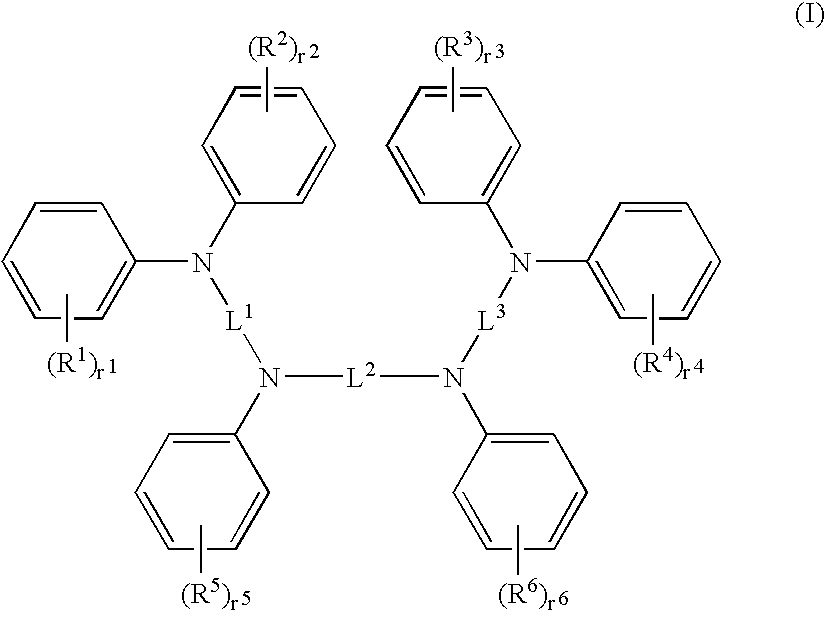
Aromatic amine derivative and organic electroluminescence device using same
a technology of organic electroluminescence and amine derivative, which is applied in the direction of organic semiconductor devices, discharge tube luminescnet screens, natural mineral layered products, etc., can solve the problems of increasing driving voltage, shortening lifetime, and low current efficiency, so as to improve the luminance and lifetime extension of organic el devices, reduce capability, and reduce the effect of current efficiency
- Summary
- Abstract
- Description
- Claims
- Application Information
AI Technical Summary
Benefits of technology
Problems solved by technology
Method used
Image
Examples
example 2 (
Synthesis of TA-6)
(1) Synthesis of 4-bromo-4′-iodobiphenyl
[0132] 50.0 g of 4-bromobiphenyl, 23.7 g of iodine, 10.6 g of ortho periodicacid, 13 ml of concentrated sulfuric acid, 400 ml of acetic acid and 45 ml of water were placed, and then they were stirred at 90° C. for 7 hours. After the reaction was completed, it was cooled down to room temperature, and then 1 liter of water was poured therein, followed by stirring for 1 hour. The precipitated solid was separated by filtration, followed by methanol washing and drying under reduced pressure, and then 68.0 g of 4-bromo-4′-iodobiphenyl as white crystal was obtained.
(2) Synthesis of 4-(N,N-diphenylamino)-4′-bromobiphenyl
[0133] 15.7 g of 4-bromo-4′-iodobiphenyl, 7.44 g of N,N-diphenylamine, 1.67 g of copper(I) iodide, 6.31 g of sodium t-butoxide, 772 mg of N,N′-dimethylethylene-diamine and 50 ml of xylene were placed, and then they were stirred for 18 hours under reflux. The resultant was cooled down to room temperature, followed...
example 3 (
Evaluation of TA-1)
[0143] A glass substrate (manufactured by GEOMATEC Company) of 25 mm×75 mm×1.1 mm thickness having an ITO transparent electrode was cleaned by application of ultrasonic wave in isopropyl alcohol for 5 minutes and then by exposure to ozone generated by ultraviolet light for 30 minutes.
[0144] The cleaned glass substrate having an ITO transparent electrode line was fixed to a substrate holder of a vacuum deposition apparatus, and on the surface, where the ITO transparent electrode line was fixed, of the substrate, a film layer having film thickness of 80 nm of TA-1 was formed so as to cover the transparent electrode. The film performs as a hole transporting layer.
[0145] Subsequently, a layer having layer thickness of 40 nm of EM1 was formed through a vapor deposition. Concurrently, as a light emitting molecule, the following amino compound D1 containing a styryl group was deposited at the ratio by weight between EM1 and D1 of 40:2 by a vapor deposition. The film pe...
example 4 (
Evaluation of TA-6)
[0148] The same procedure of Example 3 was repeated except that TA-6 in place of TA-1 was used, and the organic EL device was fabricated.
[0149] The half lifetime of the organic EL device was measured at the initial luminance of 5,000 nit, room temperature and DC constant current driving. The results are shown in Table 1.
PUM
| Property | Measurement | Unit |
|---|---|---|
| transmittance | aaaaa | aaaaa |
| work function | aaaaa | aaaaa |
| transmittance | aaaaa | aaaaa |
Abstract
Description
Claims
Application Information


