Indium Oxide-Cerium Oxide Based Sputtering Target, Transparent Electroconductive Film, and Process for Producing a Transparent Electroconductive Film

a technology of indium oxidecerium oxide and sputtering target, which is applied in the direction of cable/conductor manufacturing, insulating support layer, natural mineral layered products, etc., can solve the problems of etching residue generation, and affecting the etching effect of the wire material, etc., to achieve the effect of restricting the cell reaction

Inactive Publication Date: 2007-09-13
IDEMITSU KOSAN CO LTD
View PDF6 Cites 17 Cited by
  • Summary
  • Abstract
  • Description
  • Claims
  • Application Information

AI Technical Summary

Benefits of technology

[0084] As described above, according to the invention, a transparent electroconductive film is obtained which constitutes a transparent electrode wherein residues or the like are not generated by etching with a weak acid (such as an organic acid). Moreover, a sputtering target for producing such a transparent electroconductive film is obtained.
[0085] According to the invention, a transparent electroconductive film is obtained which constitutes a transparent electrode having resistance against an etchant for a reflective electrode when the reflective electrode over the transparent electrode is etched. Moreover, a sputtering target for produci

Problems solved by technology

However, it is necessary to crystallize ITO in order to make the specific resistance of ITO low.
However, the occurrence of the inconveniences due to the use of the strong acid may be problematic.
In other words, in a liquid crystal display device wherein constituents such as TFTs (thin film transistors) are used, metallic thin lines may be used for

Method used


Image

  • Indium Oxide-Cerium Oxide Based Sputtering Target, Transparent Electroconductive Film, and Process for Producing a Transparent Electroconductive Film

Examples


example 1

[0089] In2O3 powder having an average particle diameter of 1 μm or less and CeO2 powder having an average particle diameter of 1 μm or less were formulated to set the atom number ratio of cerium / indium to 0.012, and the resultant was put into a pot made of a resin. Furthermore, pure water was added thereto, and the components were subjected to wet ball mill mixing, using a hard ZrO2 ball mill. The mixing time was set to 20 hours.

[0090] As a result of the mixing, the resultant mixed slurry was taken out, filtrated, dried and granulated. The thus-obtained granulated product was shaped by cold isostatic press under an applied pressure of 294 MPa (3 t / cm2).

[0091] Next, the shaped body was sintered as follows:

[0092] First, in a sintering furnace, prepared was an atmosphere wherein oxygen was being introduced at a rate of 5 L / min. per 0.1 m3 of the volume of the furnace. Under this atmosphere, the shaped body was sintered at 1450° C. for 8 hours. At this time, the temperature was raise...

example 2

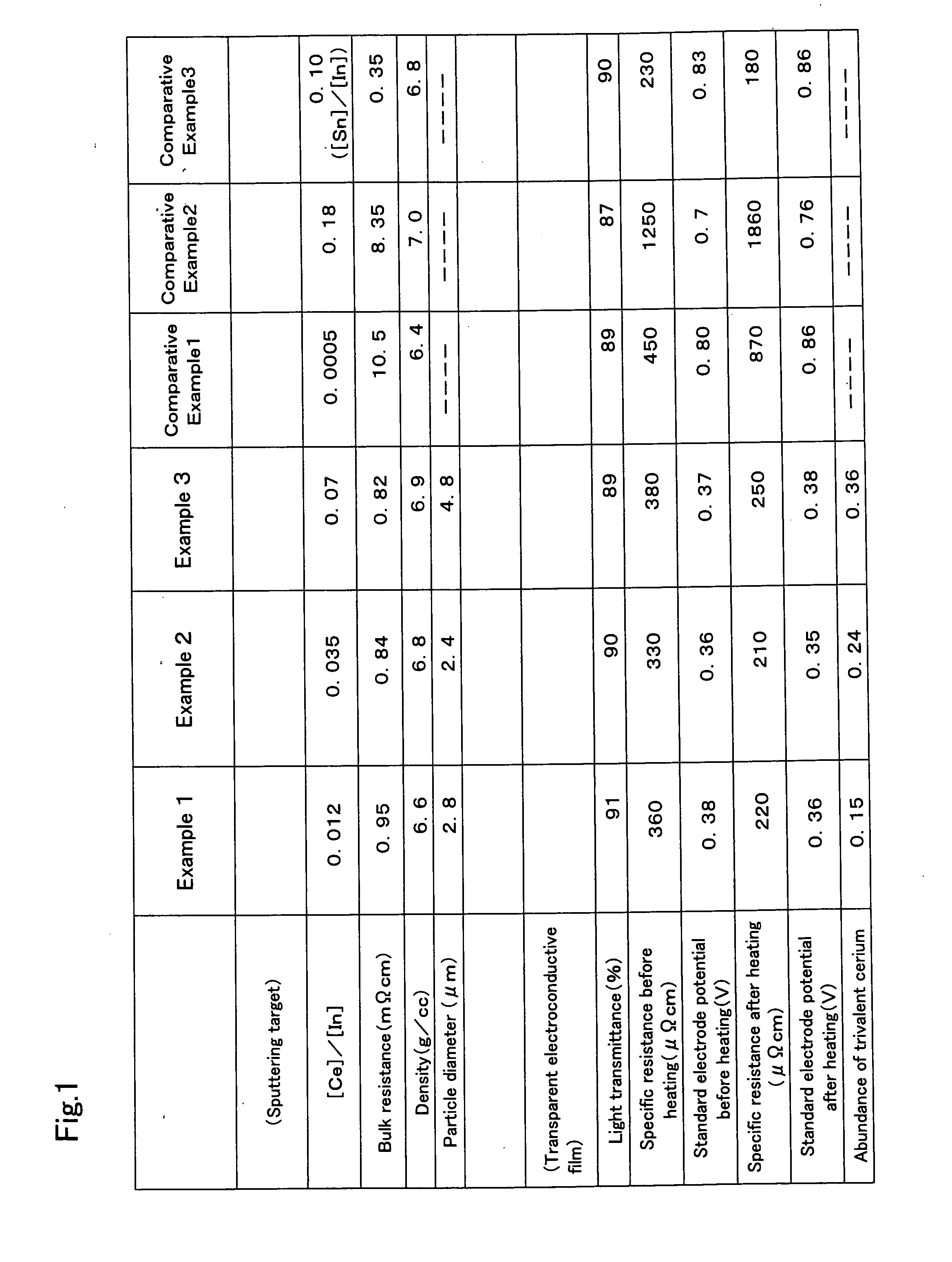
[0104] In the example 2, the same processing and operations as in above Example 1 were performed except that the ratio between the number of cerium atoms and that of indium atoms ((the number of cerium atoms) / (that of indium atoms)) per unit volume or unit mass was set to 0.035.

[0105] As a result of this processing, a cerium-containing In2O3 sintered body wherein the bulk resistance was 0.84 mΩcm, and the density was a value of 6.8 g / cc or more was obtained. The presence of cerium oxide in the sintered body could be ascertained by X-ray diffraction. The size of particles of cerium oxide that was present as a simple substance could be ascertained also with an EPMA. Cerium oxide was dispersed and contained in this manner, whereby the diameter of the crystal grains was 2.4 μm. This diameter was obtained by image processing. This sputtering target was used to form a transparent thin film having a thickness of 70 μm.

[0106] The light transmittance of the thus-obtained glass substrate wi...

example 3

[0112] In the example 3, the same processing and operations as in above Example 1 were performed except that the ratio between the number of cerium atoms and that of indium atoms ((the number of cerium atoms) / (that of indium atoms)) per unit volume or unit mass was set to 0.07.

[0113] As a result of this processing, a cerium-containing In2O3 sintered body wherein the bulk resistance was 0.82 mΩcm, and the density was a value of 6.9 g / cc or more was obtained. The presence of cerium oxide in the sintered body could be ascertained by X-ray diffraction. The size of particles of cerium oxide that was present as a simple substance could be ascertained also with an EPMA. Cerium oxide was dispersed and contained in this manner, whereby the diameter of the crystal grains was 4.8 μm. This diameter was obtained by image processing. This sputtering target was used to form a transparent thin film having a thickness of 70 μm.

[0114] The light transmittance of the thus-obtained glass substrate wit...


PUM

PropertyMeasurementUnit
Temperatureaaaaaaaaaa
Lengthaaaaaaaaaa
Diameteraaaaaaaaaa

Abstract

A transparent conductive film for constructing a transparent electrode that is free from the generation of residue, etc. by etching with a weak acid (for example, organic acid). Further, there is provided a sputtering target for producing the transparent conductive film. In particular, there is provided a sputtering target composed of indium oxide and cerium oxide, characterized in that in the observation of crystal peaks by X-ray diffractometry, the presence of peaks ascribed to indium oxide and cerium oxide is observed, and that in the EPMA measurement, the diameter of cerium oxide particles dispersed in indium oxide is measured as being ≦5 μm. A transparent conductive film is formed by a sputtering technique with the use of this sputtering target. This transparent conductive film is substantially free from the generation of residue, etc. by etching with a weak acid (for example, organic acid).

Description

BACKGROUND ART [0001] The invention relates to a sputtering target for producing an electrode substrate for driving liquid crystal, an electrode substrate for EL, or the like. The invention also relates to a transparent electroconductive film produced by use of the sputtering target, and a process for producing a transparent electroconductive film, using the sputtering target. BACKGROUND ART Technical Background [0002] Hitherto, materials doped with Sn have been investigated for a sputtering target for transparent electroconductive films. In particular, ITO (indium tin oxide) has widely been used. [0003] However, it is necessary to crystallize ITO in order to make the specific resistance of ITO low. It is therefore necessary to form ITO into a film at high temperature, or conduct predetermined thermal treatment after ITO is formed into a film. [0004] For etching process of a crystallized ITO film, aqua regia (a mixed solution of nitric acid and hydrochloric acid), which is a strong ...

Claims


Application Information

Patent Timeline
IPC IPC(8): C23C14/00C23C14/08C23C14/34G02F1/1343C23C14/58H01B5/14H01B13/00H01L21/285H01L51/50H05B33/14H05B33/28
CPCC23C14/086C23C14/3414C23C14/5806C04B35/01C04B2235/3229C04B2235/80C04B2235/5445C04B2235/6585C04B2235/6586C04B2235/77C04B2235/786C04B2235/3286C23C14/34
Inventor INOUE, KAZUYOSHIMATSUBARA, MASATOTOMAI, SHIGEKAZU
Owner IDEMITSU KOSAN CO LTD
Why Eureka
Try Eureka