Mos Capacitor And Semiconductor Device

a technology of capacitors and capacitors, applied in semiconductor devices, diodes, instruments, etc., can solve the problems of difficult for the mos capacitor to stably function as a capacitor, difficult for the mos capacitor to function as a storage capacitor, and the thickness of the insulating film used in the integrated circuit is generally large, so as to achieve uniform thickness, reduce the area of the capacitor in the integrated circuit, and increase the capacitance value per area of the capacitor

Inactive Publication Date: 2007-09-13
SEMICON ENERGY LAB CO LTD
View PDF10 Cites 34 Cited by
  • Summary
  • Abstract
  • Description
  • Claims
  • Application Information

AI Technical Summary

Benefits of technology

[0016] Further, a MOS capacitor having the aforementioned structure can use a gate insulating film as a dielectric of the capacitor. A gate insulating film is thin and has a uniform thickness as compared to other insulating films used in an integrated circuit. Therefore, when the gate insulating film is used as a dielectric, a capacitance value per area of the capacitor can be increased, and an area of the capacitor in an integrated circuit can be reduced.
[0017] In addition, since a gate insulating film has few defects or impurities and has a uniform thickness, it has an advantageous property of a high withstand voltage against dielectric breakdown regardless of its thickness. Accordingly, a MOS capacitor with high withstand voltage can be formed.
[0018] In addition, according to the semiconductor device of the present invention, a MOS capacitor having a high capacitance value per area can be formed while suppressing the number of the manufacturing steps, therefore, cost reduction can be achieved. Further, since the MOS capacitor is a non-conductive capacitor, high design flexibility of a semiconductor device can be ensured.

Problems solved by technology

Accordingly, a potential of the gate electrode and a potential of the source region or the drain region are inverted from each other at regular intervals, thus it is difficult for the MOS capacitor to stably function as a capacitor.
Also, in the case of a storage capacitor used in a pixel of a liquid crystal display device, an AC voltage is applied to the storage capacitor depending on a driving method, in which case it is difficult for the MOS capacitor to function as a storage capacitor.
However, an insulating film other than a gate insulating film used in an integrated circuit is generally thick.
Therefore, when a capacitor is formed by using such an insulating film as its dielectric, a capacitance value per area is decreased, which makes it difficult to reduce an area of the capacitor in the integrated circuit.
Further, when an insulating film as thin as a gate insulating film is formed separately to be used as a dielectric only for increasing the capacitance value of the capacitor per area, the number of the manufacturing steps of the integrated circuit is disadvantageously increased.

Method used


Image

  • Mos Capacitor And Semiconductor Device
  • Mos Capacitor And Semiconductor Device
  • Mos Capacitor And Semiconductor Device

Examples


embodiment 1

[0058] In this embodiment, description is made on an example where the MOS capacitor of the present invention is used as a storage capacitor in a pixel of a liquid crystal display device.

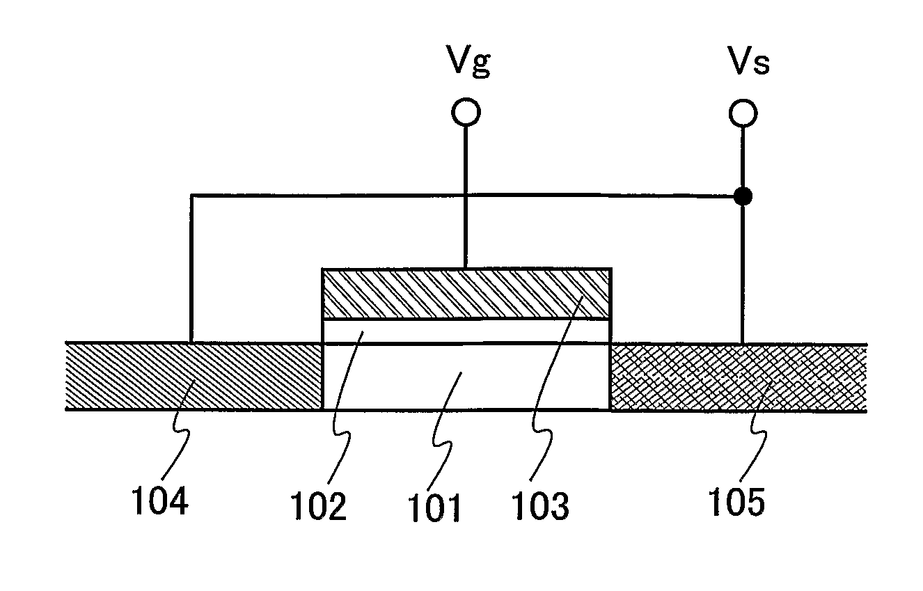
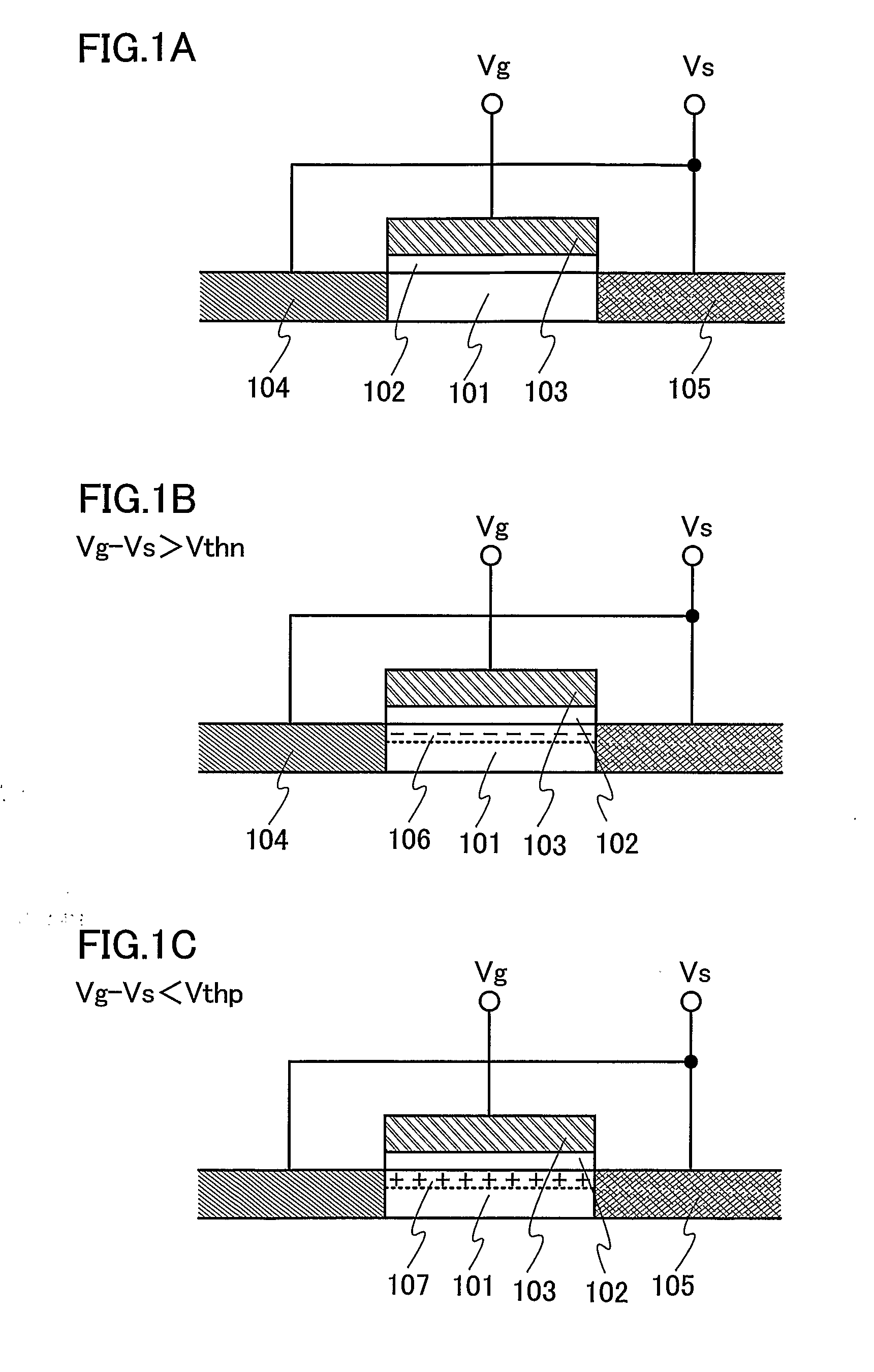
[0059]FIG. 5 is a block diagram illustrating a configuration of a liquid crystal display device. In FIG. 5, reference numeral 701 denotes a pixel portion, 702 denotes a scan line driver circuit and 703 denotes a signal line driver circuit. In the pixel portion 701, a plurality of pixels 704 are arranged in matrix. Note that FIG. 5 illustrates only one pixel 704. The pixel 704 comprises a TFT 705 functioning as a switching element, a liquid crystal cell 706 and a storage capacitor 707. The liquid crystal cell 706 includes a pixel electrode, a counter electrode and a liquid crystal interposed between them.

[0060] In the pixel portion 701, a signal line 708 and a scan line 709 are formed. A gate electrode of the TFT 705 is connected to the scan line 709. One of a source region and a drain region of th...

embodiment 2

[0069] The MOS capacitor of the present invention can also be used as a capacitor that is connected to an antenna for constructing a resonant circuit in a semiconductor device such as an ID chip and an IC chip capable of wireless data communication (e.g., identification of data). Note that the ID chip is also referred to as a wireless tag, an RFID (Radio Frequency IDentification) tag, an IC card and a wireless chip. Each of the ID chip, the IC card and the wireless chip comprises an antenna and an integrated circuit.

[0070] The ID chip and the IC card can communicate with a reader / writer by utilizing radio waves. Specifically, the ID chip and the IC card can transmit signals to the reader / writer by operating an integrated circuit using an AC voltage, which is generated in an antenna by radio waves generated from the reader / writer, and modulating signals generated in the antenna using signals outputted from the integrated circuit.

[0071]FIG. 6 is a block diagram illustrating an exemp...

embodiment 3

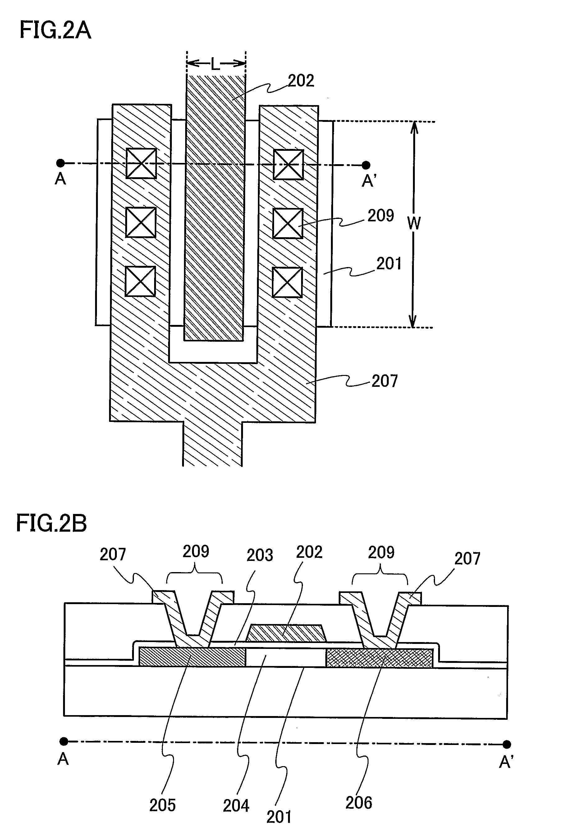
[0078] Description is made below on a specific manufacturing method of an ID chip as one mode of the semiconductor device of the present invention. In this embodiment, TFTs and a MOS capacitor are shown as exemplary semiconductor elements, however, semiconductor elements used in an integrated circuit are not limited to these. For example, memories, diodes, photoelectric converters, resistors, coils or inductors can be used as the semiconductor elements.

[0079] First, as shown in FIG. 7A, a peeling layer 501 is formed over a heat-resistant first substrate 500. The first substrate 500 may be a glass substrate such as barium borosilicate glass and alumino borosilicate glass, a quartz substrate, a ceramic substrate and the like. Alternatively, it may be a metal substrate including a stainless (SUS) substrate or a semiconductor substrate. Generally, a substrate formed of a flexible synthetic resin such as plastics tends to have a low heat-resistance temperature as compared to the aforeme...


PUM

PropertyMeasurementUnit
thicknessaaaaaaaaaa
thicknessaaaaaaaaaa
thicknessaaaaaaaaaa

Abstract

A capacitor capable of functioning as a capacitor even when an AC voltage is applied thereto is provided without increasing the manufacturing steps of a semiconductor device. A transistor is used as a MOS capacitor where a pair of impurity regions formed on opposite sides of a channel formation region are each doped with impurities of different conductivity so as to be used as a source region or a drain region. Specifically, assuming that an impurity region that is doped with N-type impurities is referred to as an N-type region while an impurity region that is doped with P-type impurities is referred to as a P-type region, a transistor is provided where a channel formation region is interposed between the N-type region and the P-type region, which is used as a MOS capacitor.

Description

TECHNICAL FIELD [0001] The present invention relates to a capacitor using a transistor, and a semiconductor device using such a capacitor. BACKGROUND ART [0002] A capacitor is one of the essential passive elements for manufacture of a semiconductor integrated circuit (hereinafter abbreviated to an integrated circuit), particularly an analog circuit. Specifically, it is used as a storage capacitor in a pixel of a liquid crystal display device as well as an analog circuit such as a power supply circuit and a DRAM. Increase in the area of a capacitor leads to a higher cost of an integrated circuit, therefore, it is preferable that the capacitor occupy a small area but have a large capacitance value. [0003] A gate insulating film of a transistor is advantageous in that it is thin and has a uniform thickness as compared to other insulating films used in an integrated circuit, has few defects or impurities, and has a high withstand voltage against dielectric breakdown in spite of its thic...

Claims


Application Information

Patent Timeline
Patent Type & Authority Applications(United States)
IPC IPC(8): H01L27/108G02F1/1362G02F1/1368H01L21/288H01L21/3205H01L21/336H01L21/768H01L21/77H01L21/822H01L21/8234H01L21/8242H01L21/84H01L27/04H01L27/06H01L27/08H01L27/12H01L27/13H01L29/04H01L29/786
CPCG02F1/136213H01L21/288H01L21/32051H01L21/76801H01L21/76829H01L21/76838H01L29/78675H01L27/10805H01L27/1214H01L27/1266H01L27/13H01L29/04H01L27/0811H10B12/30H10B12/00
Inventor KATO, KIYOSHISHIONOIRI, YUTAKA
Owner SEMICON ENERGY LAB CO LTD
Why Eureka
Try Eureka