

Ceramic coating member for semiconductor processing apparatus
- Summary
- Abstract
- Description
- Claims
- Application Information
AI Technical Summary
Benefits of technology
Problems solved by technology
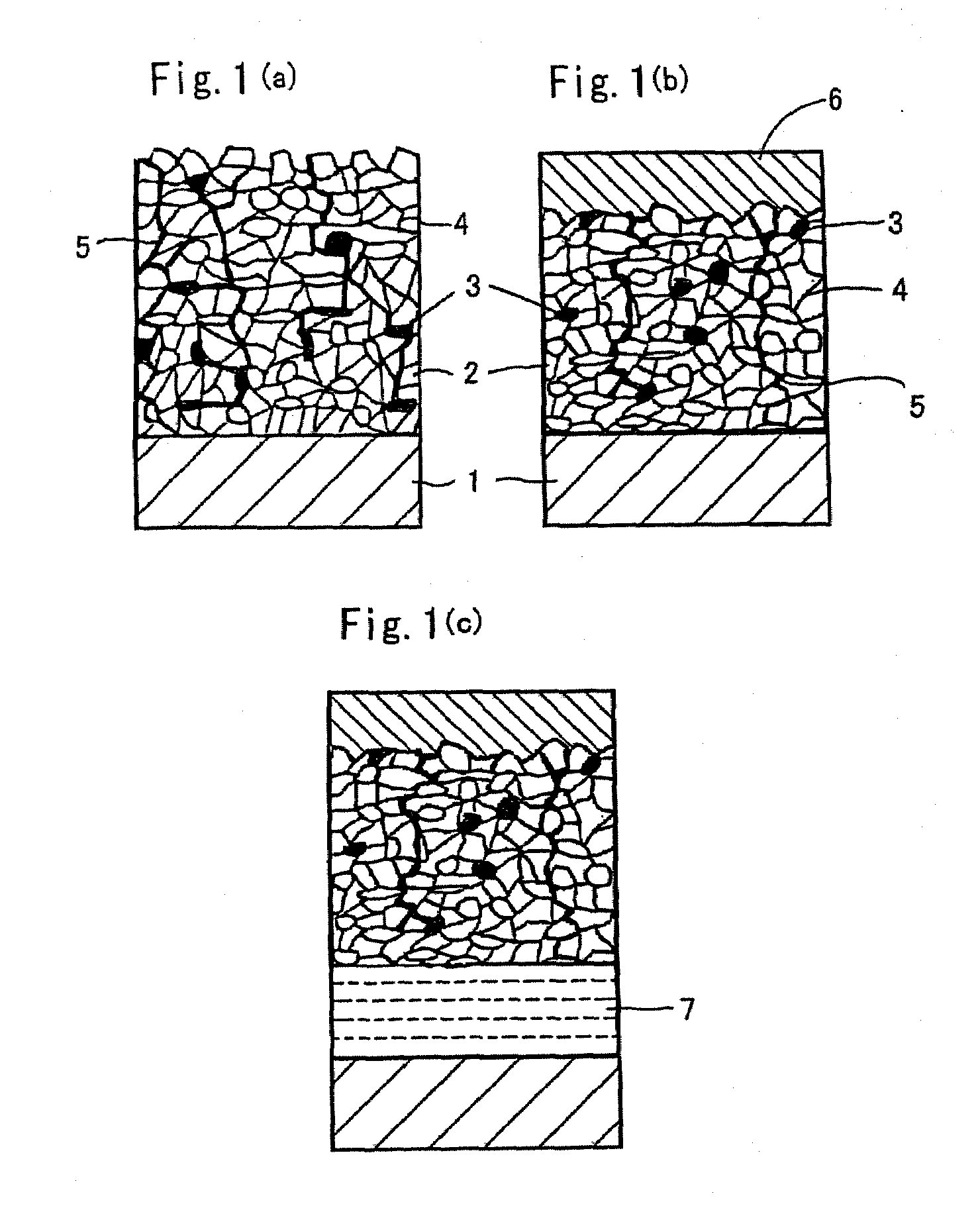
Method used
Image

Examples
example 1
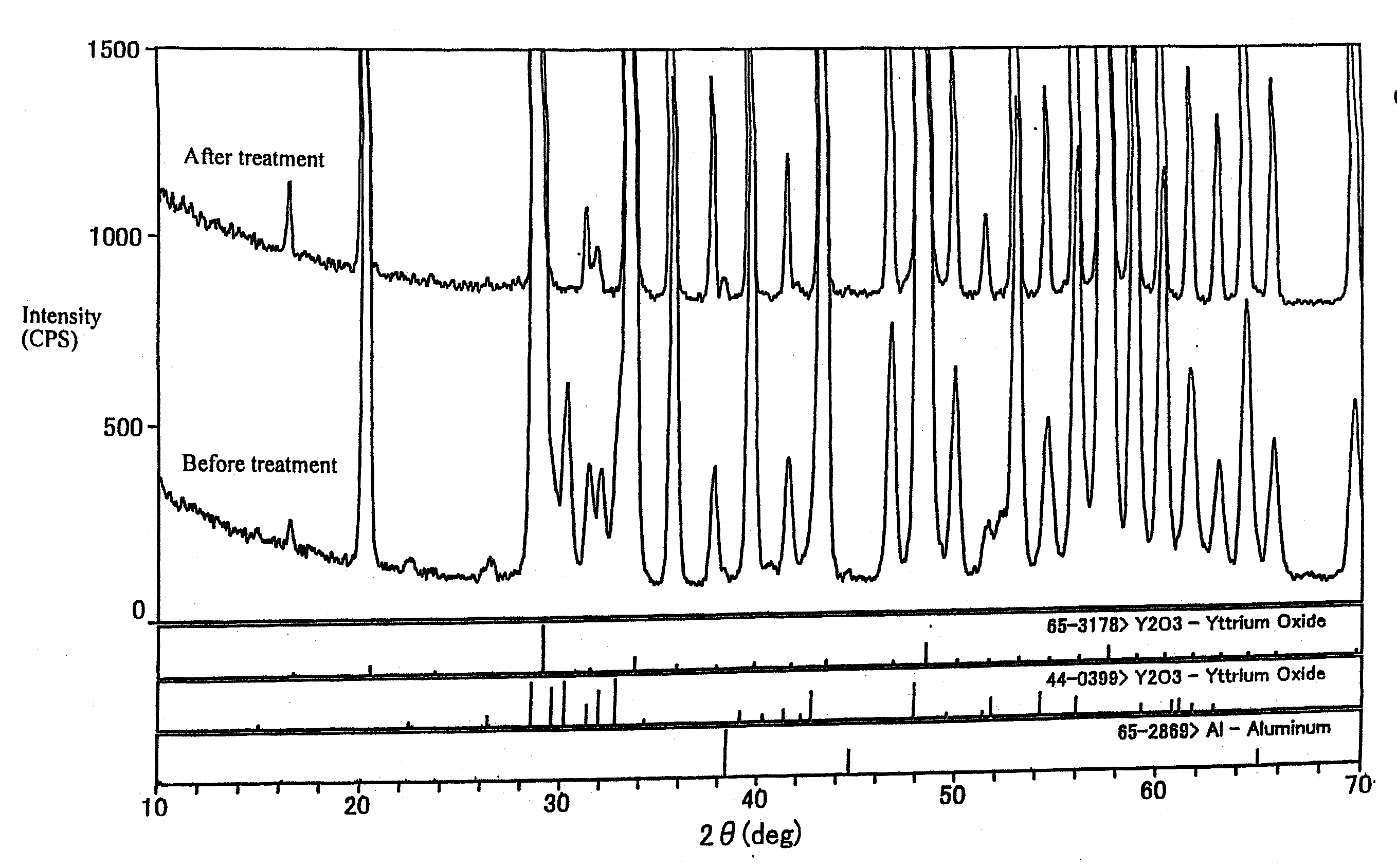
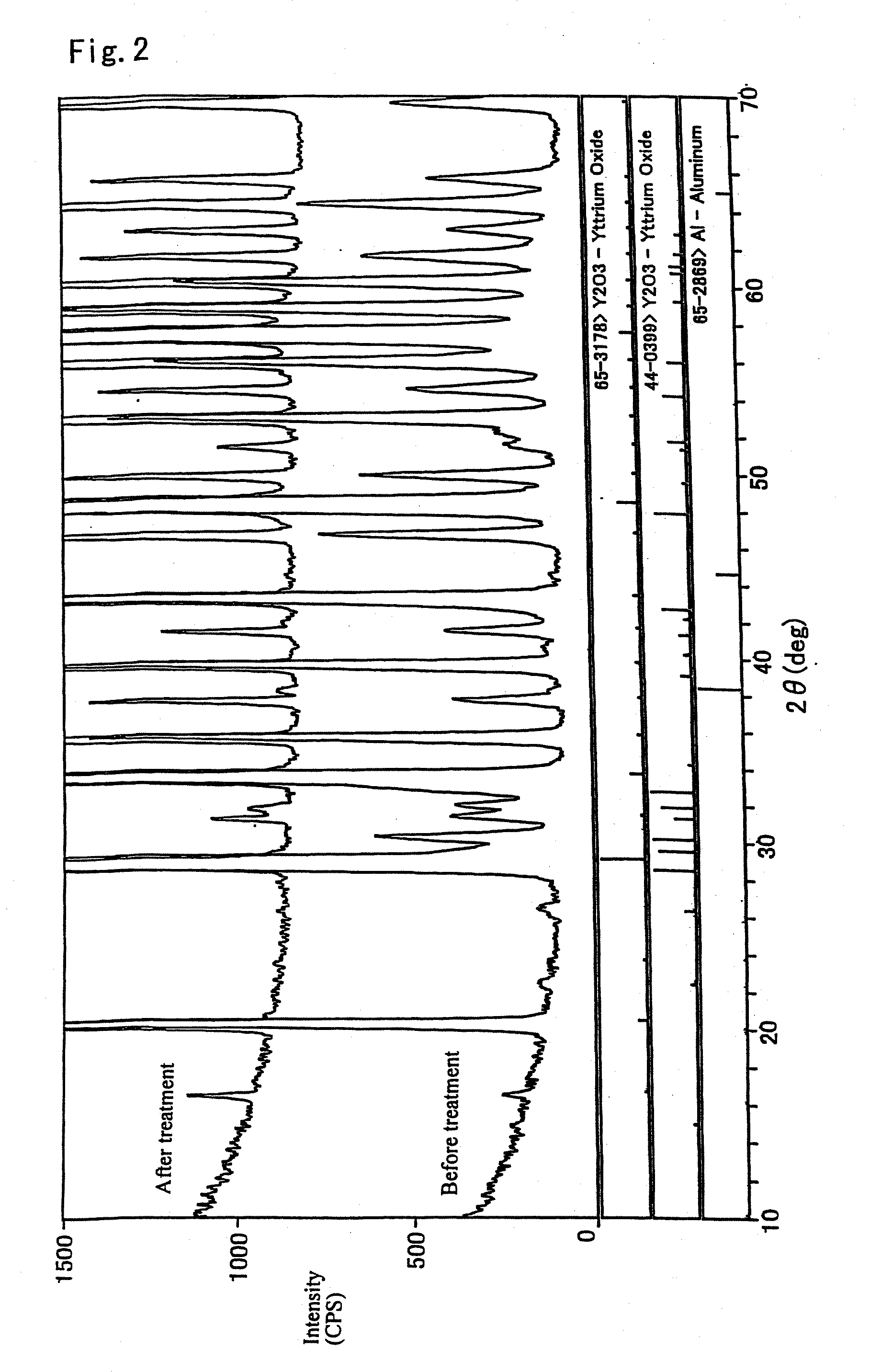
[0077]In this example, an undercoat (spray coating) of 80 mass % Ni-20 mass % Cr is formed on a surface of an Al substrate (size: 50 mm×50 mm×5 mm) by an atmospheric plasma spraying method and a porous coating is formed thereon with powders of Y2O3 and CeO2 by the atmospheric plasma spraying method, respectively. Thereafter, the surfaces of the spray coating are subjected to two kinds of high energy irradiation treatments, i.e. electron beam irradiation and laser beam irradiation. Then, the surface of the thus obtained coating to be tested is subjected to a plasma etching work under the following conditions. The number of particles of coating element scraped and flying from the coating through the etching treatment is measured to examine the resistance to plasma erosion and the resistance to environmental contamination. The comparison is conducted by measuring a time that 30 particles having a particle size of 0.2 μm or more adhere to the surface of a silicon wafer of 8 inches in di...
example 2
[0088]In this example, a coating is formed by spraying a film-forming material as shown in Table 3 onto a surface of an Al substrate having a size of 50 mm×100 m×5 mm. Thereafter, a part of the coating is subjected to an electron beam irradiation treatment for forming a secondary recrystallized layer suitable for the invention. Then, a specimen having a size of 20 mm×20 mm×5 mm is cut out from the resulting treated coating and is masked so as to expose an area of 10 mm×10 mm, which is subjected to a plasma irradiation under the following conditions, and thereafter an amount damaged through plasma erosion is measured by means of an electron microscope or the like.
(1) Gas atmosphere and flowing condition
CF4 / Ar / O2=100 / 1000 / 10 ml (flow amount per 1 minute)
(2) Plasma irradiation output
[0089]High frequency power: 1300 W
Pressure: 133.3 Pa
[0090]The above results are summarized in Table 3. As seen from the results of this table, all of the anodized coating (No. 8), B4C spray coating (No. 9) ...
example 3
[0096]In this example, the resistance to plasma erosion in the coating formed by the method of Example 2 before and after the electron beam irradiation treatment is examined. As a specimen to be tested, ones obtained by directly forming the following mixed oxide onto an Al substrate at a thickness of 200 μm through an atmospheric plasma spraying method are used.
(1) 95% Y2O3-5% SC2O3
(2) 90% Y2O3-10% Ce2O3
(3) 90% Y2O3-10% Eu2O3
[0097]Moreover, the electron beam irradiation and gas atmosphere element after the film formation, plasma irradiation conditions and the like are the same as in Example 2.
[0098]The above results are summarized in Table 4 as an amount damaged through plasma erosion. As seen from the results of this table, the coatings of oxides in Group IIIA of the Periodic Table under the conditions adaptable for the invention are better in the resistance to plasma erosion even in the use at the mixed oxide state as compared with the Al2O3 (anodizing) and B4C coatings disclos...
PUM
| Property | Measurement | Unit |
|---|---|---|
| Length | aaaaa | aaaaa |
| Fraction | aaaaa | aaaaa |
| Thickness | aaaaa | aaaaa |
Abstract
Description
Claims
Application Information