Resist pattern forming method, thin-film pattern forming method, and microdevice manufacturing method

a technology of resist pattern and forming method, which is applied in the direction of photosensitive material processing, photomechanical equipment, instruments, etc., can solve the problems of insufficient achievement of conventional relacs method, and achieve the effect of high density

Inactive Publication Date: 2007-10-25
TDK CORPARATION
View PDF4 Cites 40 Cited by
  • Summary
  • Abstract
  • Description
  • Claims
  • Application Information

AI Technical Summary

Benefits of technology

[0017]These thin-film pattern forming methods of the present invention can manufacture a sufficiently fine thin-film pattern by using a resist pattern having a sufficiently narrow trench width formed by the above-mentioned method of the present invention as a mask pattern.
[0018]The present invention a

Problems solved by technology

However, it has recently been demanded to form a resist pattern having a further narrower

Method used


Image

  • Resist pattern forming method, thin-film pattern forming method, and microdevice manufacturing method
  • Resist pattern forming method, thin-film pattern forming method, and microdevice manufacturing method
  • Resist pattern forming method, thin-film pattern forming method, and microdevice manufacturing method

Examples


examples

[0063]The present invention will now be explained more specifically.

[0064]Preparation of Resin Composition

[0065]A resin composition was obtained by adding 20 g of pure water to 160 g of an aqueous solution containing 5 wt % of polyvinyl acetal KW3 manufactured by Sekisui Chemical Co., Ltd., 20 g of an aqueous solution containing about 10 wt % of (N-methoxymethyl)methoxyethyleneurea, 20 g of (N-methoxymethyl)hydroxyethyleneurea, and 20 g of N-methoxymethylurea, and stirring and mixing them for 6 hr at room temperature.

[0066]The aqueous solution containing 5 wt % of polyvinyl acetal KW3 was obtained by adding 400 g of pure water to 100 g of an aqueous solution containing 20 wt % of polyvinyl acetal resin S-LEC KW3, and stirring and mixing them for 6 hr at room temperature by using a 1-L measuring flask. The aqueous solution of (N-methoxymethyl)methoxyethyleneurea was obtained by adding 860 g of pure water and 40 g of IPA (isopropanol) to 100 g of (N-methoxymethyl)methoxyethyleneurea, ...

examples 1 to 6

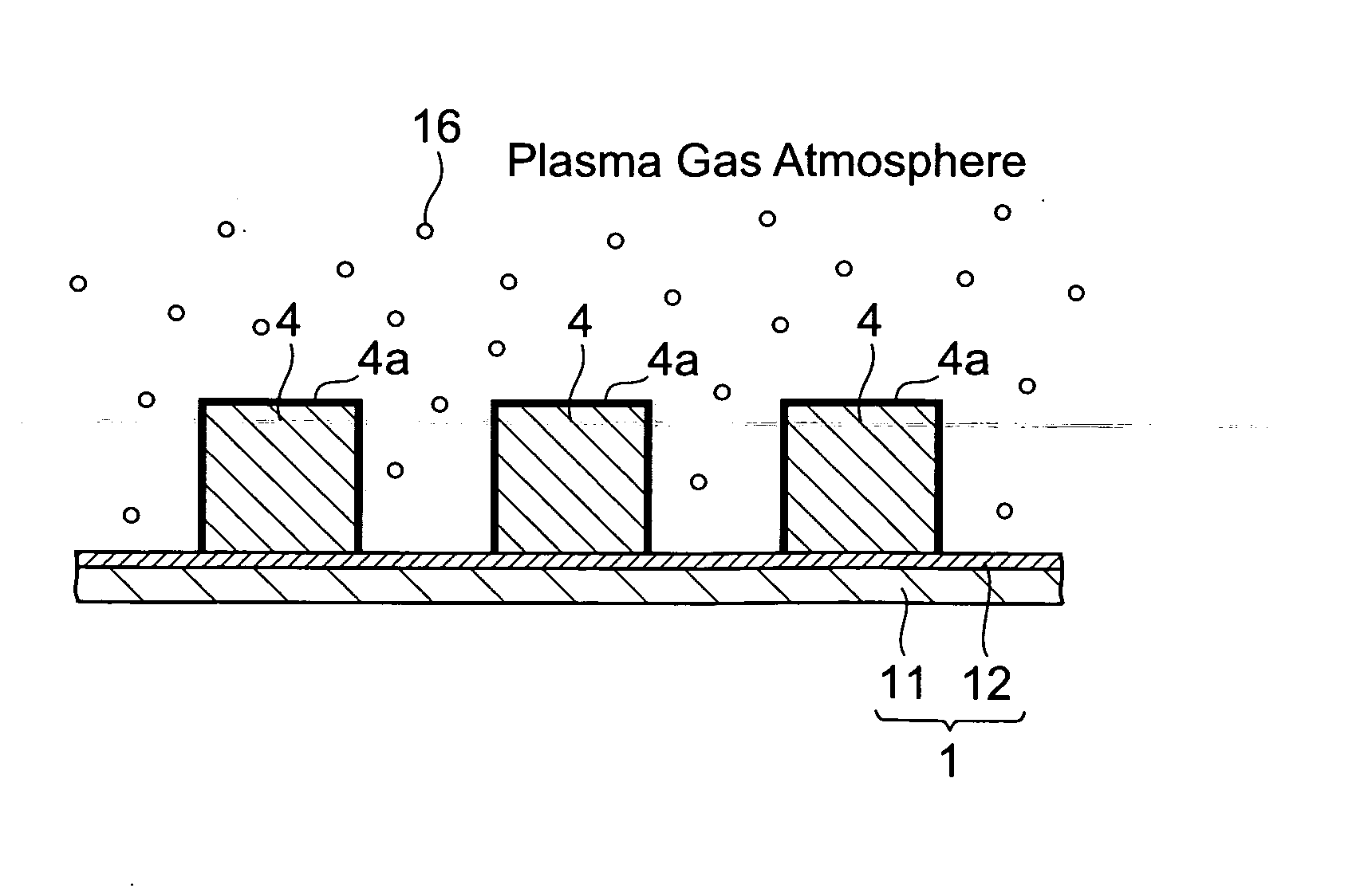
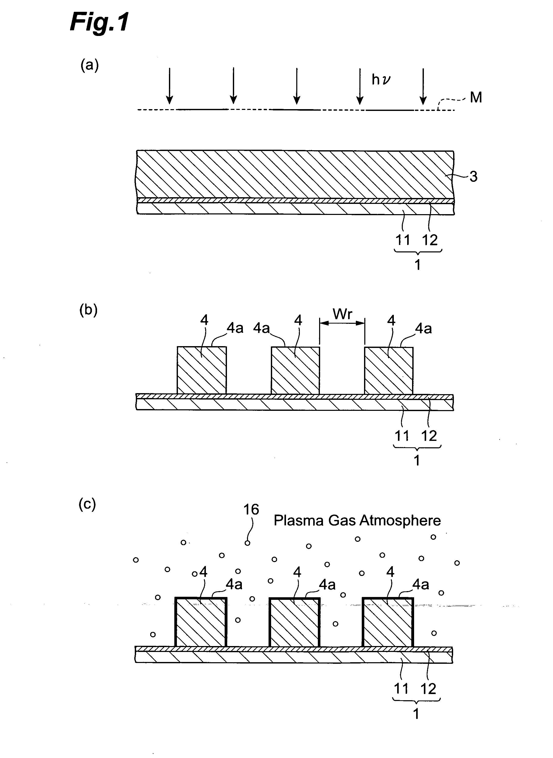
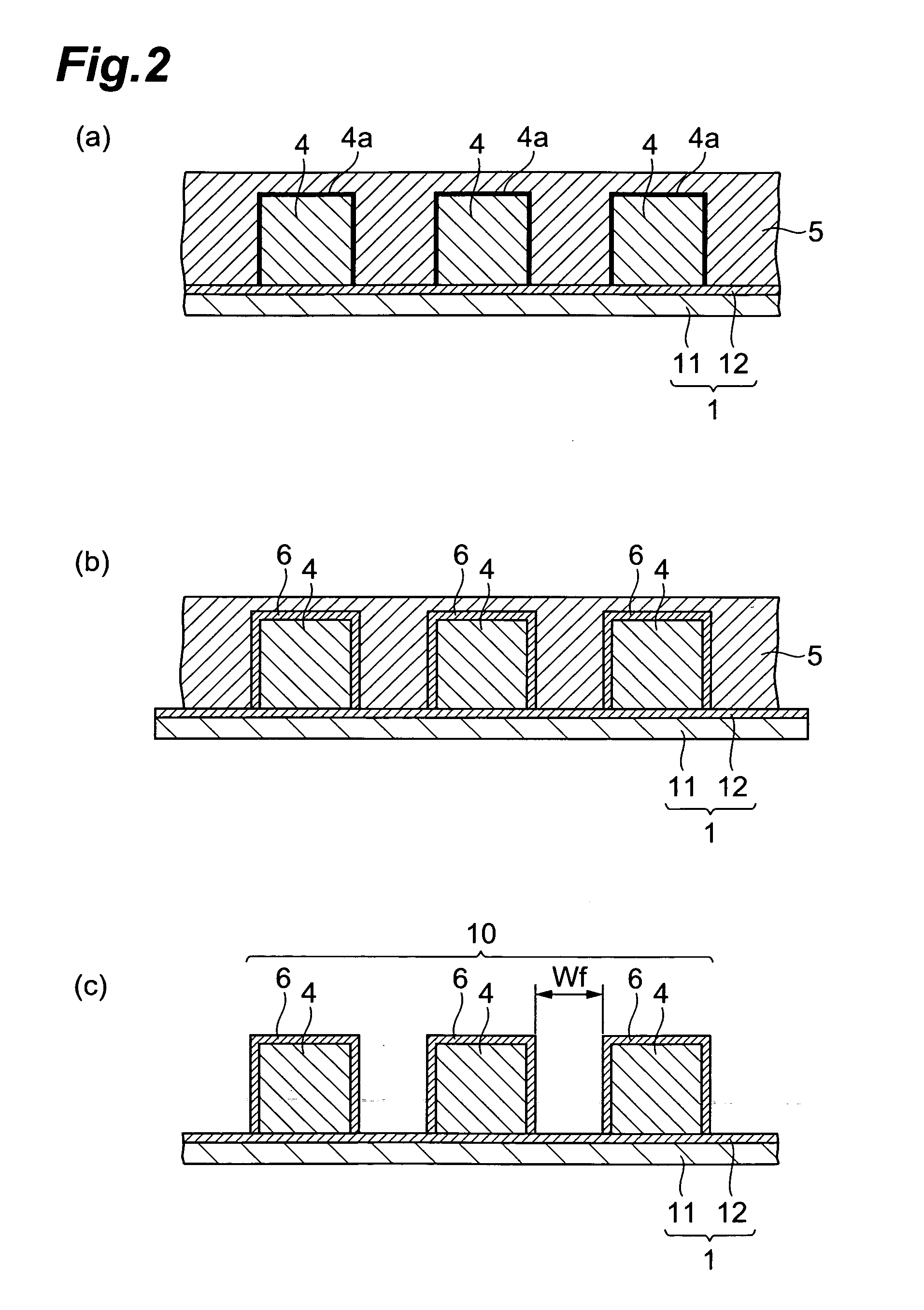
[0067]A thin film of Ni (having a thickness of 100 nm) was formed by sputtering on a surface of an Si substrate having a diameter of 6 inches, so as to yield a substrate (hereinafter referred to as “Ni substrate”) comprising the Si substrate and Ni thin film. Then, a patterned resist layer was formed on the Ni substrate as follows:

[0068]Chemically-amplified polyhydroxystyrene-based resist AZ DX5105P (product name; manufactured by AZ Electronic Materials Co., Ltd.), which was a resist for a wavelength of 248 nm (KrF excimer laser) and contained an acid-generating material adapted to generate an acid upon heating, was applied by spin-coating onto the Ni substrate such as to yield a thickness of 500 nm after prebaking. The applied resist was prebaked by heating for 90 sec at 100° C. by a hotplate, then cooled to room temperature by a cooling plate, and thereafter exposed to light through a mask by using a DUV stepper (NSR-EX14D (product name) manufactured by Nikon Corp., NA=0.65, σ=0.7...


PUM


Abstract

A resist pattern forming method comprises the steps of plasma-processing a surface of an acid-feedable resist layer formed and patterned on a surface of a substrate in a gas atmosphere containing a fluorocarbon; attaching a resin composition crosslinkable in the presence of an acid to the plasma-processed surface of the resist layer; crosslinking the resin composition in a part in contact with the resist layer by feeding an acid from the resist layer, so as to form a crosslinked layer covering the resist layer; and removing the resin composition from a part excluding the crosslinked layer, so as to yield a resist pattern comprising the resist layer and the crosslinked layer covering the resist layer.

Description

BACKGROUND OF THE INVENTION[0001]1. Field of the Invention[0002]The present invention relates to a resist pattern forming method, a thin-film pattern forming method, and a microdevice manufacturing method.[0003]2. Related Background Art[0004]In recent years, studies for making thin-film patterns finer have been underway in order to attain a higher density in microdevices having thin films such as thin-film magnetic heads, semiconductor devices, and MEMS devices. Its typical example is a method using a resist pattern which will be explained in the following.[0005]First, a resist layer is formed on a thin film. This layer is exposed to light through a photomask, and is developed with an alkaline developer, so as to form a resist pattern. Finally, the thin film in the part not covered with the resist pattern is removed by dry etching or the like; or a plating layer is deposited thereon, then the resist pattern is removed, and the thin film in the part not covered with the plating layer...

Claims


Application Information

Patent Timeline
IPC IPC(8): G03F7/26
CPCG03F7/40G11B5/3116H01L21/32139H01L21/0273H01L21/31144G11B5/3163
Inventor KAMIJIMA, AKIFUMI
Owner TDK CORPARATION
Why Eureka
Try Eureka