Method for producing gallium nitride light emitting diode wafer

a technology of light-emitting diodes and gallium nitride, which is applied in the direction of basic electric elements, electrical apparatus, and semiconductor devices, can solve the problems of poor thermal stability, contact impedance, and unfavorable electric current traverse between the contact surface and the inside of the wafer, and achieves the effect of reducing contact impedance, high electrical conductivity, and good conductivity of the wafer

Inactive Publication Date: 2007-11-01
PODIUM PHOTONICS GUANGZHOU
View PDF2 Cites 3 Cited by
  • Summary
  • Abstract
  • Description
  • Claims
  • Application Information

AI Technical Summary

Benefits of technology

[0009]The advantages and effects of the present invention are that in comparison with the prior art, the magneto sputtering method uses magnetic-induced lattice deposit to contact metal, so that the conductive metal will be evenly distributed all over the surface and the inside of the contact metal, thereby achieving high electrical conductivity. The conductivity and luminous efficiency of the wafer will thus be better. This will simultaneously reduce the contact impedance of P-type luminous zone and enhance the traverse of electric current, thereby attaining an eventual equilibrium of contact impedance and luminous efficiency and thus increasing the life span of the wafer. The P-type ohmic contact layer made by zinc oxide is different from the conventional P-type contact luminous layer made by nickel and gold (Ni / Au) or indium tin oxide (ITO). It has better thermal stability and light emitting efficiency and is a new kind of lighting contact material for light emitting diode wafer. Meanwhile, conducting thermal treatment under the aforesaid conditions can slow down the speed of metal oxidation, so that every layer of metal particles will be in their most stable phase and the best performance of light transmittance and traverse of electric current will eventually be achieved. Experiments prove that by adaptation of the technical proposal of the present invention it is possible to control the decay of light intensity of gallium nitride light emitting diode in 1000 hours to less than 10%, and it possesses good thermal stability with the contact impedance being reduced to 2E-6 Ω-cm2, which provides a stable and reliable core component for solid-state lighting of semi-conductor.

Problems solved by technology

Gold is the most commonly used material for electrodes, but it has a poor thermal stability at the temperature of 500 degree Celsius or above.
Accordingly, this method can reduce contact impedance but is unfavourable to the traverse of electric current on the contact surface and the inside of the wafer.
This causes heat emission owing to localized surge of electric current, thereby reducing luminous efficiency of the wafer.
However, with the miniaturization and integration of devices, there are even more stringent requirements on the stability and reliability of ohmic contacts of gallium nitride light emitting diodes.

Method used


Image

  • Method for producing gallium nitride light emitting diode wafer
  • Method for producing gallium nitride light emitting diode wafer
  • Method for producing gallium nitride light emitting diode wafer

Examples


first embodiment

[0016]The first embodiment is detailed as follows:

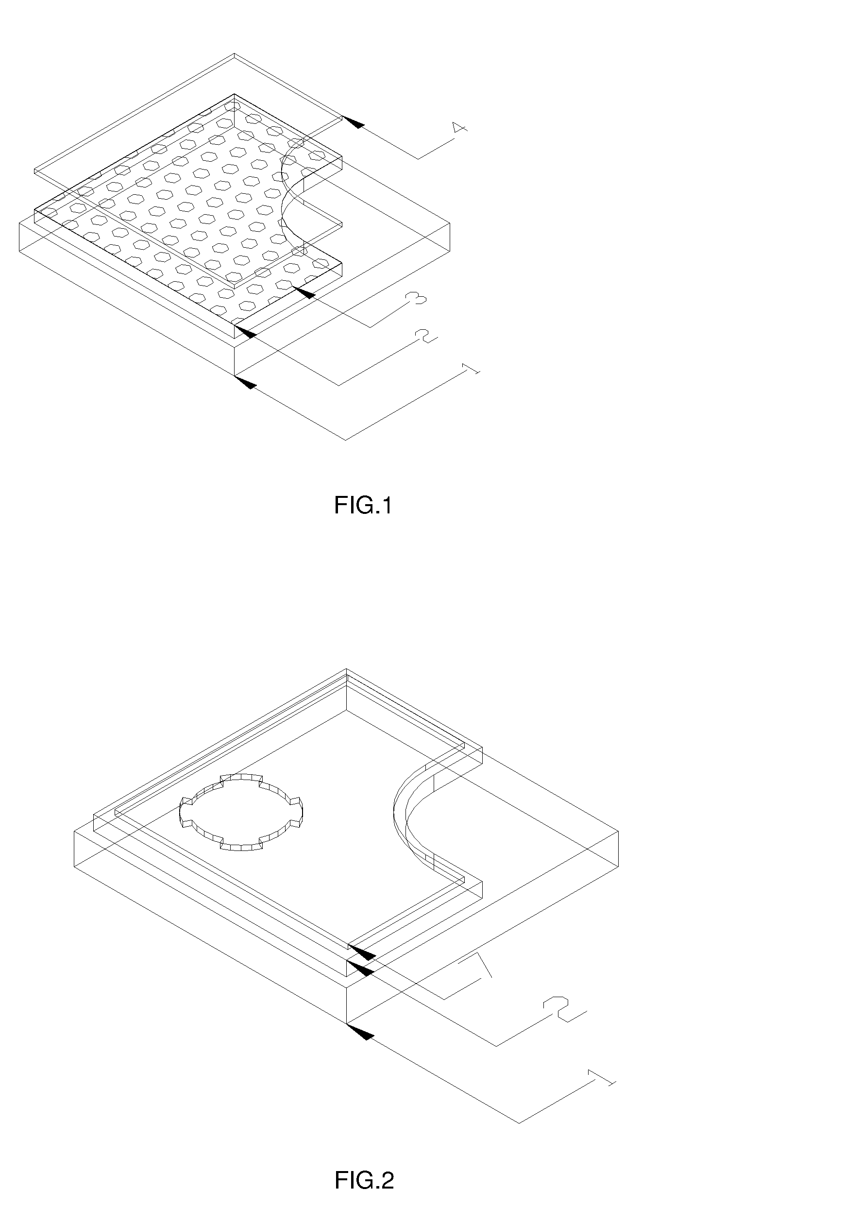
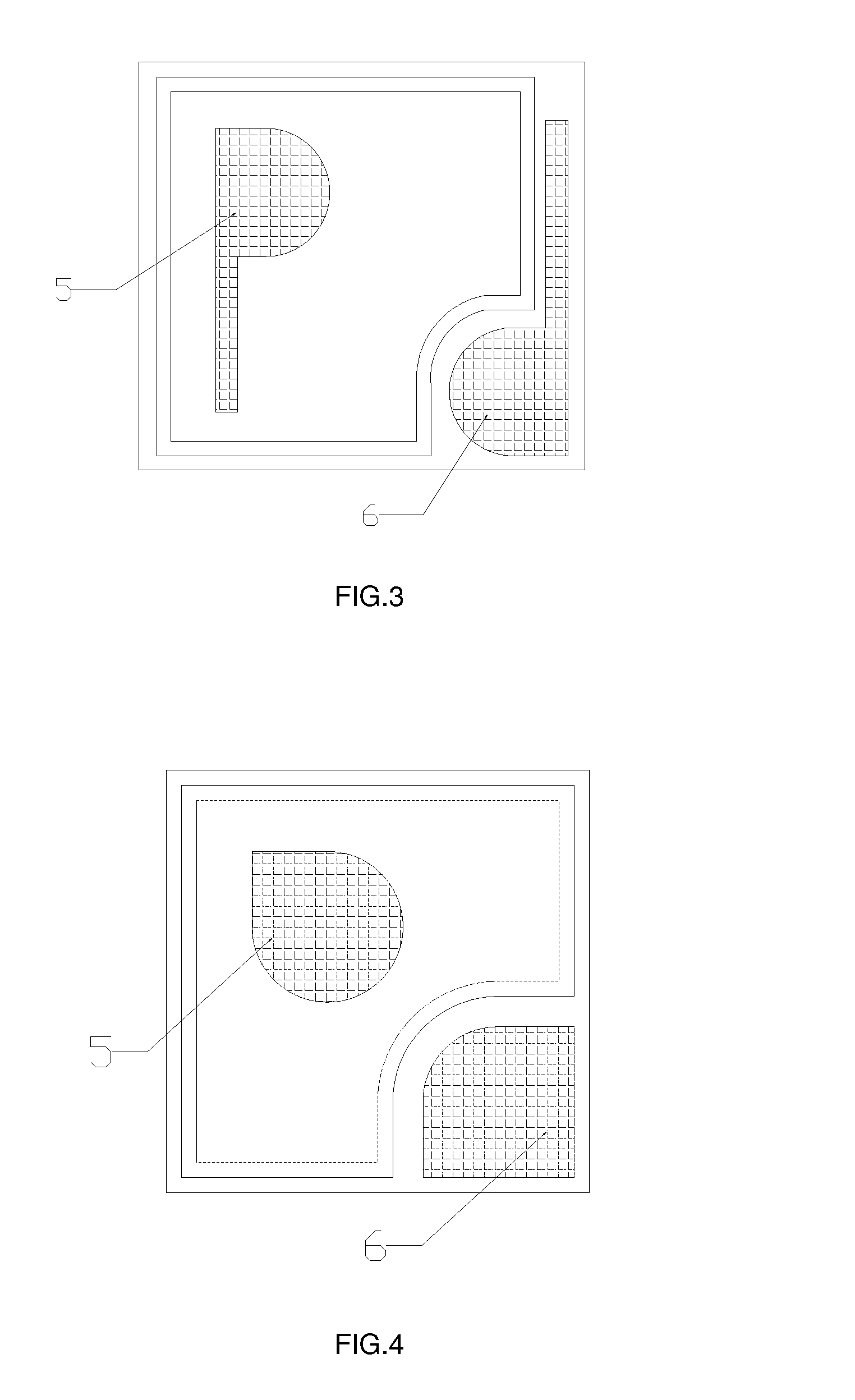
[0017]As illustrated in FIG. 1, gallium nitride epitaxial wafer 2 is developed on sapphire substrate 1. Applying the magnetic feature of nickel metal, sputtering system is used to spray nickel material in nano particles onto the surface of gallium nitride epitaxial wafer 2. The thickness of the nickel metal 3 is between 1 nanometer to 100 nanometers. Following that, apparatus such as electron-beam apparatus is used to deposit at least one layer of high work function metal film such as gold, platinum, palladium, chromium and so forth onto the surface of the nickel metal 3. Gold metal 4 is used in this embodiment. The thickness of gold and that of nickel metal 3 shall satisfy the ratio of 1:0.5˜4, so that the light output ratio and thermal stability are optimized for the same types of materials. Certainly, the composition of the first layer of electrode metal can also be: nickel / platinum; nickel / palladium; chromium, nickel / gold; nickel...

second embodiment

[0020]The second embodiment is detailed as follows:

[0021]As illustrated in FIG. 2, the difference between this embodiment and the first embodiment is that zinc oxide 7 is used as the first layer of electrodes. The P-type ohmic contact layer made by zinc oxide is different from the conventional P-type contact luminous layer made by indium tin oxide or by nickel and gold in the first embodiment. It has better thermal stability and light emitting efficiency and is a new kind of lighting contact material for light emitting diode wafer. By way of epitaxies (including MOCVD, GPE, MBE and so forth), a layer of oxide of zinc metal, namely zinc oxide 7, is grown on the gallium nitride epitaxial wafer, or by way of production methods (including E-BEAM, SPUTTER and so forth), zinc oxide 7 is evaporated, thereby the light transmittance of the wafer can reach 95% or above and the contact impedance and thermal stability can achieve the same performance as the conventional nickel and gold. Besides...


PUM

PropertyMeasurementUnit
thicknessaaaaaaaaaa
light transmittanceaaaaaaaaaa
thicknessaaaaaaaaaa

Abstract

The present invention relates to a method for improving the performance of P-type ohmic contact of gallium nitride LED wafer. Magneto sputtering is used to spray nickel material in nano particles onto the surface of gallium nitride epitaxial layer. The thickness of nickel is between 1 nm to 100 nm. Following that, at least one layer of high work function metal film is deposited onto the surface of the nickel metal layer, and the ratio of the thickness of the nickel metal layer to that of high work function metal film is 1:0.5˜4. Zinc oxide may replace nickel metal layer and high work function metal film. The object of the present invention is to simultaneously reduce the contact impedance of P-type luminous zone and enhance the traverse of electric current, thereby attaining an eventual equilibrium of contact impedance and luminous efficiency and thus increasing the life span of the wafer. The present invention prescribes the thickness ratio for each contact metal layer, the conditions of thermal treatment and the unique design patterns for electrodes. Experiments prove that the present invention is able to control the decay of light intensity of gallium nitride LED in 1000 hours to less than 10% with good thermal stability and contact impedance being reduced to 2E-6 Ω-cm2.

Description

BACKGROUND OF THE INVENTION[0001]The present invention relates to a method for producing gallium nitride light emitting diode wafer and more particularly pertains to a method for improving the performance of P-type ohmic contact of gallium nitride light emitting diode wafer.[0002]Gallium nitride light emitting diode is a light emitting diode of ultra high brightness. It is widely used in sectors such as communications, transportation and displays as it has the features of being energy-saving, pollution-free, durable, small in size and producing shape colors. In recent years, a large volume of research work has been conducted on the development and improvement of P-type ohmic contacts of light emitting diodes with many structures being invented which basically satisfy the requirements for a functional device. For a conventional P-type ohmic contact of light emitting diode wafer, electron-beam evaporation apparatus is usually used to deposit on the surface of an epitaxial wafer one or...

Claims


Application Information

Patent Timeline
Patent Type & Authority Applications(United States)
IPC IPC(8): H01L21/00H01L33/00H01L33/32H01L33/40
CPCH01L33/0095H01L33/40H01L33/32
Inventor WANG, MENGYUANCHEN, GUOCONG
Owner PODIUM PHOTONICS GUANGZHOU
Why Eureka
Try Eureka