Eureka AIR delivers breakthrough ideas for toughest innovation challenges, trusted by R&D personnel around the world.

Light-Assisted Electrochemical Shunt Passivation for Photovoltaic Devices

Inactive Publication Date: 2007-11-08
UNIVERSITY OF TOLEDO
View PDF21 Cites 21 Cited by
  • Summary
  • Abstract
  • Description
  • Claims
  • Application Information

AI Technical Summary

Benefits of technology

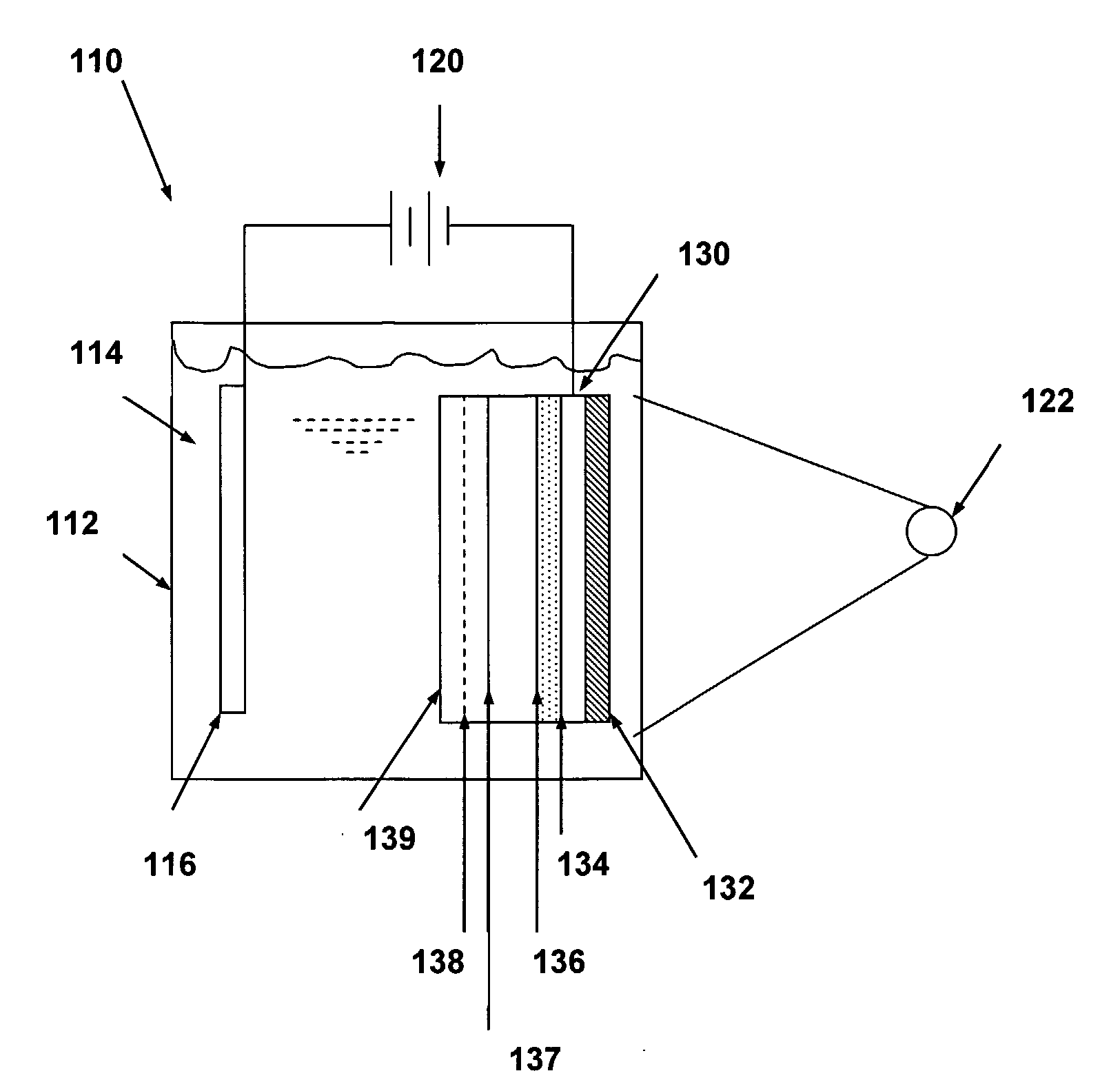
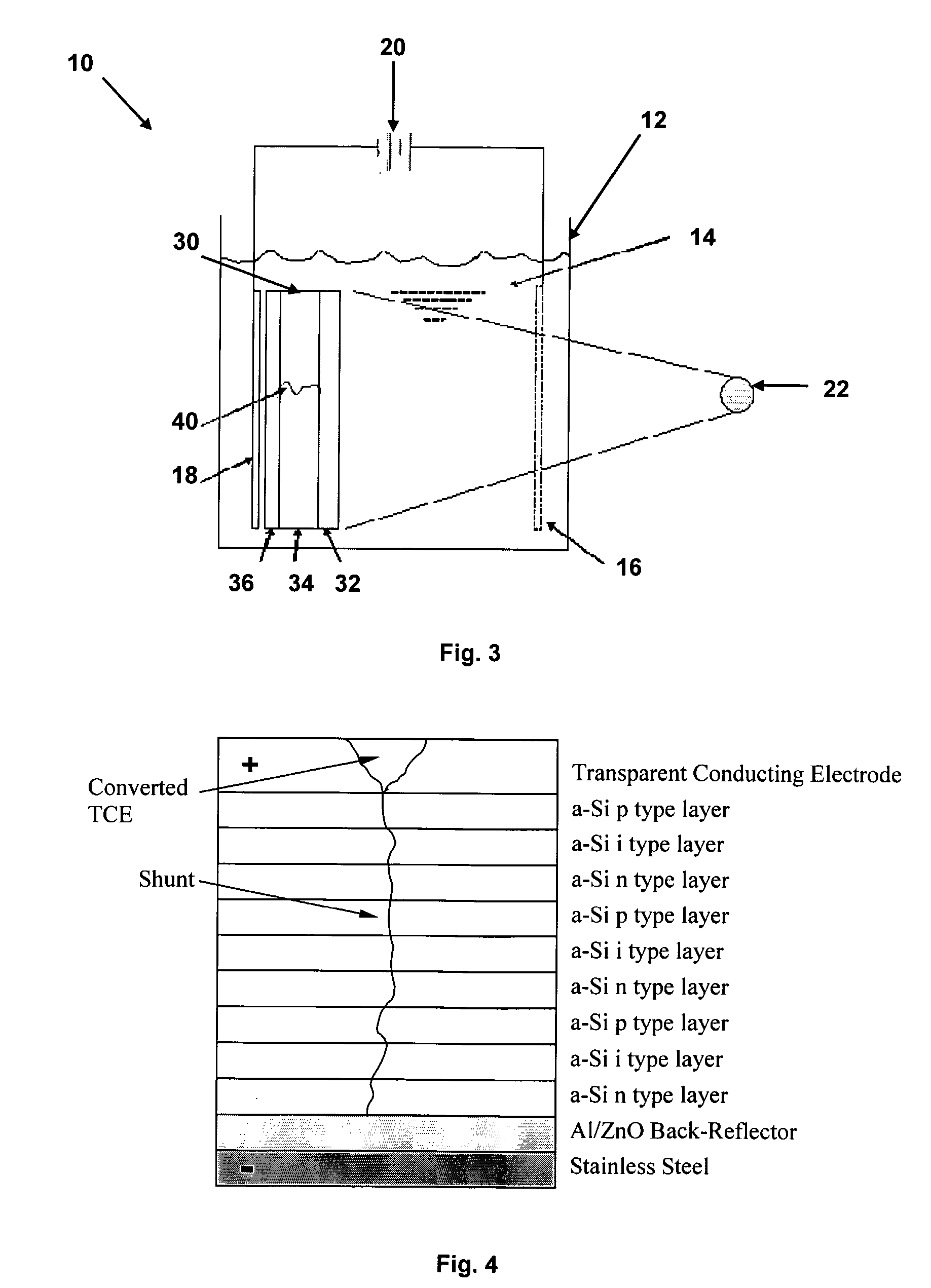
[0022] The present invention provides an improved method of eliminating or reducing the effects of short circuit (shunt) defects in a-Si photovoltaic devices, or other photovoltaic devices having a transparent conducting oxide (TCO) as the top layer.
[0028] The passivation reaction is much more selective when the cell is illuminated, because the unshunted portions of the cell produce a voltage that actively opposes the one required for the passivation to take place. This increases the acceptable range of the electrical bias for effective shunt passivation and the process passivates shunts with different levels of severity without causing unwanted conversion of the transparent conducting electrode (TCE) into a more electrically resistive material in the unshunted areas.
[0030] Therefore, a broad range of possible shunts can be effectively passivated using the method of the present invention.

Problems solved by technology

However, in the fabrication of semiconductor materials and photovoltaic devices by glow discharge, or other chemical vapor deposition processes, the presence of current-shunting, short circuit defects has been noted.
These defects seriously impair the performance of the photovoltaic devices fabricated therefrom and also detrimentally affect production yield.
These process-related defects are thought to either be present in the morphology of the substrate electrode, or to develop during the deposition or subsequent processing of the semiconductor layers.
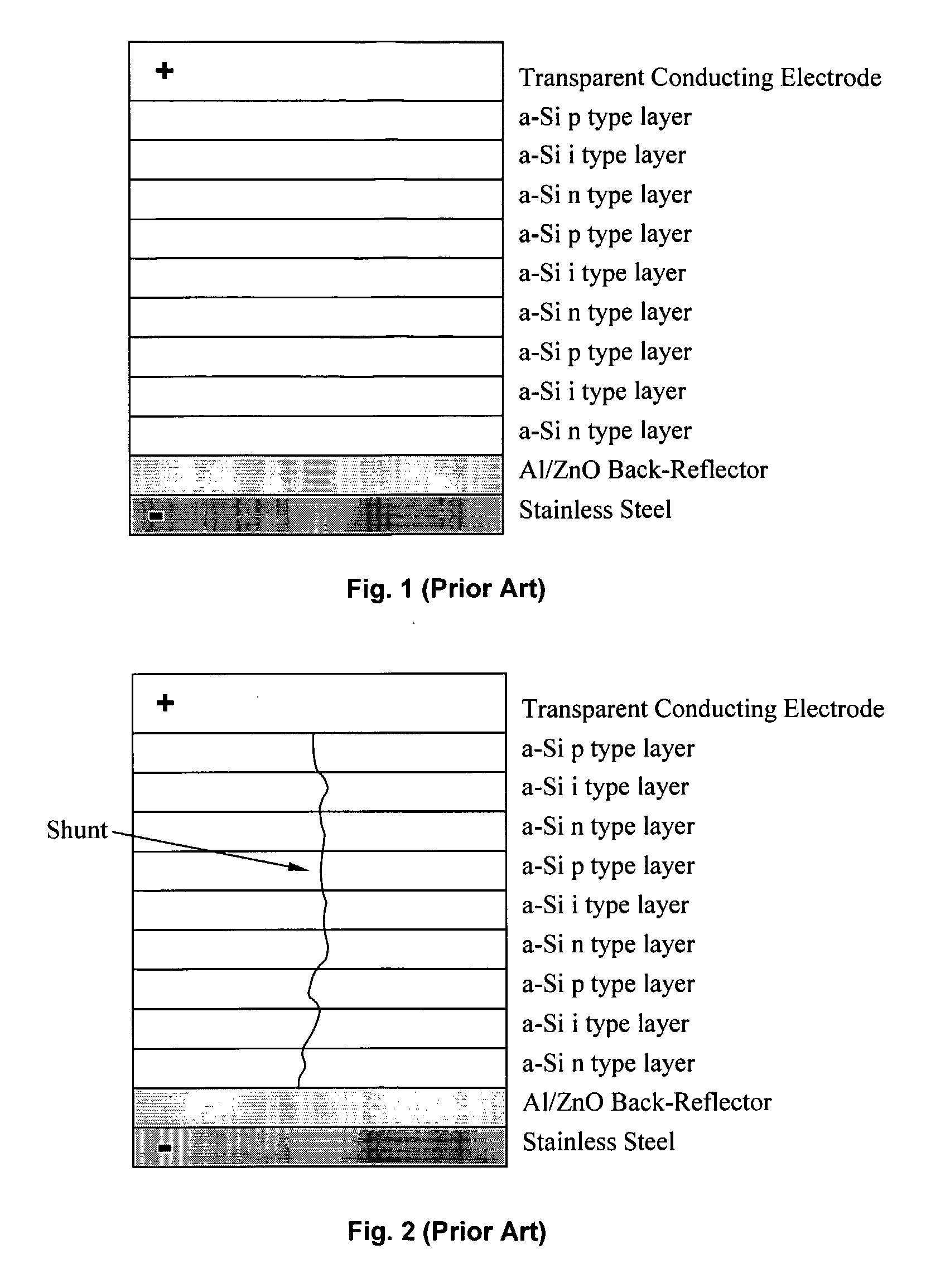
Shunt defects are present in photovoltaic devices when one or more low resistance current paths develop through the semiconductor body of the device, allowing current to pass unimpeded between the electrodes thereof.
Under operating conditions, a photovoltaic device in which a shunt defect has developed, exhibits either (1) a low power output, since electrical current collected at the electrodes flows through the defect region (the path of least resistance) in preference to an external load, or (2) complete failure where sufficient current is shunted through the defect region to “burn out” the device.
'674 described that, however, this is not possible with the reverse bias condition; and as a result, for detecting the presence and location of a short circuit current path, reverse bias is preferred.
Kawakami et al. stated that the application of too high a voltage, however, tends to cause side reactions at portions other than the short-circuit portion to be treated.
However, the inventors herein have found that the rate of the passivation reaction is unacceptably slow, at least for triple-junction amorphous silicon solar cells using ITO as the front contact, if light alone is used to generate the electrical bias.
This leads to a severe reduction in yield and performance of the solar cells.

Method used


Image

  • Light-Assisted Electrochemical Shunt Passivation for Photovoltaic Devices
  • Light-Assisted Electrochemical Shunt Passivation for Photovoltaic Devices
  • Light-Assisted Electrochemical Shunt Passivation for Photovoltaic Devices

Examples


example i

[0076]FIG. 5a is a graph showing the current-voltage characteristics of a shunted a-Si triple junction solar cell, before shunt passivation, for a first material, GD1065-1.

[0077]FIG. 5b is a graph showing the current-voltage characteristics of the same solar cell, after shunt passivation, for a first material, GD1065-1.

[0078] FIGS. 5(a) and 5(b) show one example of the shunt passivation performed by the method described herein on an amorphous silicon triple junction solar cell.

[0079]FIG. 5(a) shows the dark and illuminated current-voltage characteristics of the cell before shunt passivation. The curves indicate that the cell has a low shunt resistance, and consequently a low room light open circuit voltage, low fill factor and low efficiency. Such a cell is generally considered “dead”.

[0080]FIG. 5(b) shows the current-voltage characteristics of the same cell after shunt passivation. The fill factor increased from 26% to 56% and the efficiency from 1.3% to 6.7%. Open circuit volt...

example ii

[0081]FIG. 5c is a graph showing the current-voltage characteristics of a shunted a-Si triple junction solar cell, before shunt passivation, for a second material, GD1065-3.

[0082]FIG. 5d is a graph showing the current-voltage characteristics of the same solar cell, after shunt passivation, for a second material, GD1065-3.

[0083] FIGS. 5(c) and 5(d) show the current-voltage curves for another triple junction amorphous silicon cell before and after shunt passivation. FIG. 5(c) shows the current-voltage characteristics of a severely shunted triple junction solar cell. FIG. 5(d) shows the current voltage characteristics of the same cell after shunt passivation. All cell parameters recovered to normal values.

[0084] For both these examples the method of the present invention was used for shunt passivation. A 2 volt, 5 second pulse was applied to the solar cell. Aqueous AlCl3 was used as an electrolyte and illumination was from a tungsten halogen lamp.

example iii

[0085]FIGS. 6a, 6b, 6c and 6d are graphs showing a comparison of the results produced by the method of the present invention (“light”) with those produced by the Nath et al. process (U.S. Pat. No. 4,729,970) (“dark”) on a set of amorphous silicon solar cells. Each point on the graphs is an average of data from three separate samples. The graphs show the relative improvement in the open circuit voltage under AM1 (FIG. 6a), under 5% illumination (“room light”) (FIG. 6b), efficiency (FIG. 6c), and fill factor (FIG. 6d) for both processes, and at different applied electrical biases. The graphs show that there is at least one electrical bias at which the process described here outperforms the prior art process of Nath et al.

[0086] FIGS. 6 (a) through (d) indicate that by using the Nath et al. process (“Dark”), some samples show good improvement, but some samples actually deteriorate relative to their state before shunt passivation. With the process described in the present invention (“L...


PUM

PropertyMeasurementUnit
Timeaaaaaaaaaa
Electrical conductivityaaaaaaaaaa
Electric potential / voltageaaaaaaaaaa

Abstract

A method of passivating current-shunting defects in a photovoltaic device and such passivated photovoltaic devices are described. The photovoltaic device includes a thin film body with a superposed electrode comprised of a layer of transparent electrically conductive electrode material. The method includes converting the transparent, electrically conductive electrode material to a material having a higher electrical resistivity than the transparent electrically conductive electrode material or by removing the transparent conducting electrode material, by simultaneously: 1) immersing at least a portion of the electrode in a conversion reagent, 2) illuminating the immersed electrode with a suitable source of illumination, and 3) applying an appropriate electrical bias to activate the conversion.

Description

CROSS-REFERENCE TO RELATED APPLICATIONS [0001] This application claims the benefit of U.S. Provisional Application No. 60 / 563,132, filed Apr. 16, 2004, the disclosure of which is incorporated herein by reference.[0002] This invention was made with Government support under AFRL-Kirtland “Lightweight and flexible thin film solar cells based on amorphous silicon and cadmium telluride” under contract F29601-02-C-0304 and National Renewable Energy Laboratory “High efficiency and high rate deposited amorphous silicon solar cells” under contract NDJ-2-30630-08. The government has certain rights in this invention.FIELD OF THE INVENTION [0003] The present invention is generally directed to solar cells (photovoltaic devices) in general, and particularly to a process for passivating or isolating short circuit current paths which form in amorphous / microcrystalline silicon thin film photovoltaic devices. BACKGROUND OF THE INVENTION [0004] Photovoltaic devices that include the use of thin film am...

Claims


Application Information

Patent Timeline
IPC IPC(8): H01L31/00H01L27/14H01L31/075H01L31/18
CPCH01L31/076Y10T29/53135Y02E10/548H01L31/1868H01L31/208Y02P70/50
Inventor VIJH, AAROHIDENG, XUNMING
Owner UNIVERSITY OF TOLEDO
Why Eureka
Eureka Blog
Learn More