Semiconductor device

a technology of semiconductors and semiconductors, applied in the field of semiconductor devices, can solve the problems of contaminated wafers, difficult to implement laser programming for failure repair and others after packaging, and faulty whole packages, etc., and achieve the effect of low current consumption and small occupation area

Active Publication Date: 2007-12-06
RENESAS ELECTRONICS CORP
View PDF2 Cites 62 Cited by
  • Summary
  • Abstract
  • Description
  • Claims
  • Application Information

AI Technical Summary

Benefits of technology

[0022]An object of the invention is to provide a fuse program circuit that is formed of an electric fuse element of an interconnection blowing type that operates with a small occupation area and low current consumption.

Problems solved by technology

When a laser beam is to be used for programming such fuse elements, a laser apparatus for the fuse programming is required, and a step of transporting wafers from an inspection apparatus to the laser apparatus is necessary, resulting in problems such as wafer contamination.
Therefore, it is difficult to implement the laser programming for failure repairing and others after packaging.
For example, when an SIP is formed of an inexpensive chip and an expensive chip stacked each other, if a fault is found in the inexpensive chip after packaging, the whole package becomes faulty, and the expensive chip is also treated as a faulty chip.
Since the LT fuse is physically cut by the externally applied laser beam, the apparatus dedicated to trimming and the repairing step are required as already described, and the increase in cost due to investment on the apparatus as well as increase in TAT (Turn-Around Time) are unavoidable.
Therefore, it is difficult to reduce the occupation area of the fuse circuit including the fuse elements.
However, Reference 1 discloses, as the fuse elements, only the LT fuse elements that can be blown through application of the laser beam, and Reference 1 does not consider fuse elements that can be electrically blown off.
Although Reference 3 discloses the blowing of the fuse elements with the current, it does not disclose any specific layout of the fuse elements, power consumption and others.
However, the flash memory is used, and a circuit construction for the programming is large, resulting in a problem that a fixed information program circuit of a small occupation area cannot be achieved without difficulty.

Method used


Image

  • Semiconductor device
  • Semiconductor device
  • Semiconductor device

Examples


first embodiment

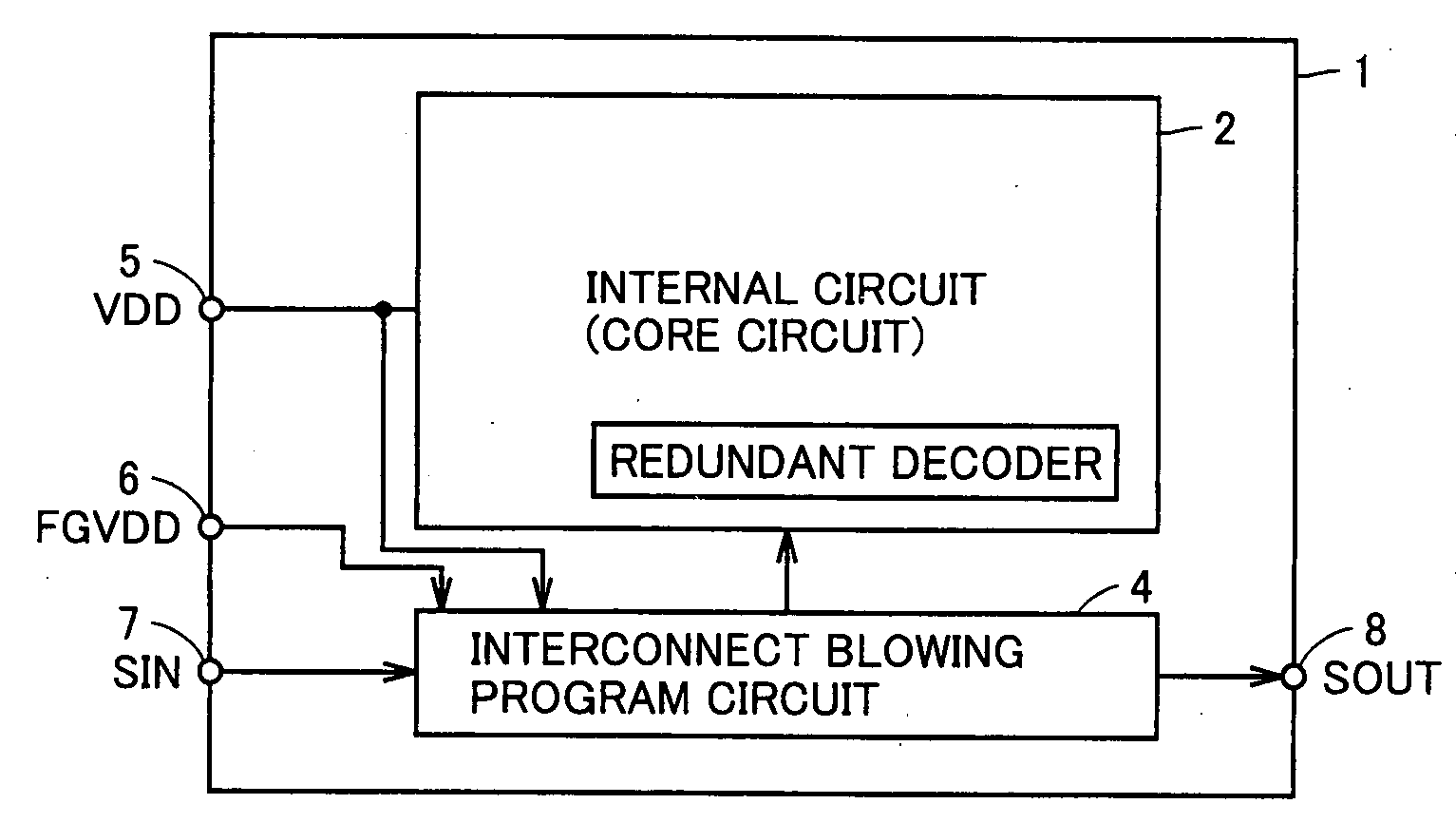
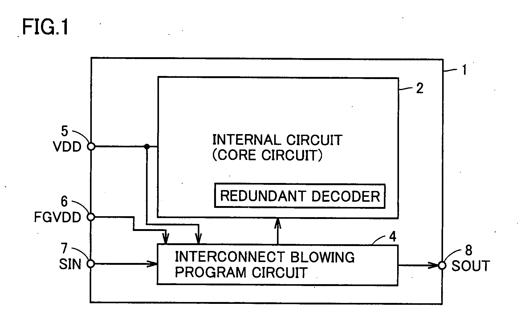
[0072]FIG. 1 schematically shows a whole construction of a semiconductor device according to a first embodiment of the invention. In FIG. 1, a semiconductor integrated circuit device 1 includes an internal circuit (core circuit) 2 implementing a predetermined function, and an interconnect blowing program circuit 4 for fixedly storing an operation state of internal circuit 2 or information defining the operation state (the information related to the internal circuit).

[0073]This semiconductor integrated circuit device 1 may be formed on a semiconductor chip singly, or may be integrated with another function block such as a processor or a memory on the same chip.

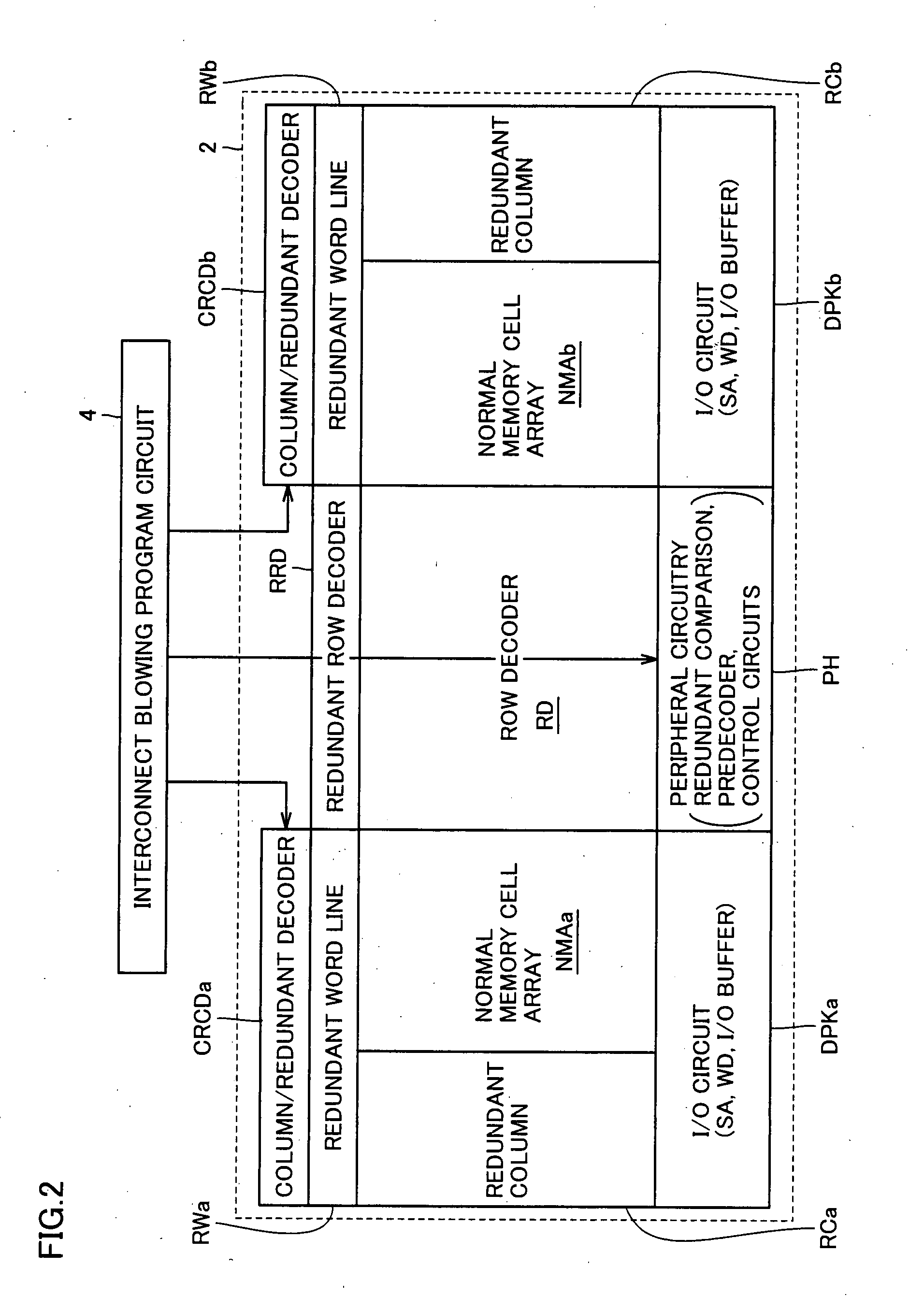
[0074]Internal circuit 2 receives, as an operation power supply voltage, a power supply voltage VDD from a power supply node 5, and implements a predetermined function. Internal circuit 2 is a core circuit of the semiconductor integrated circuit device, and it may be a memory circuit including a memory cell array, or may also b...


PUM


Abstract

In fuse program circuits, fuse element FS is implemented using metal interconnect at third or higher layer of multilayer metal interconnect. In each fuse program circuit, program information and fuse select information are sequentially transferred using a scan flip-flops, and fuses are selectively and electrically blown one by one. The fuse program circuit provided with fuse elements that can be programmed even after packaging is implemented with low power consumption and a low occupation area.

Description

BACKGROUND OF THE INVENTION[0001]1. Field of the Invention[0002]The present invention relates to a semiconductor device having a fuse program circuit that includes a fuse element storing fixed information, and particularly to a construction for implementing a fuse program circuit operating with low power consumption and small occupation area.[0003]2. Description of the Background Art[0004]Fuse program circuit is employed in semiconductor integrated circuit devices for various purposes. The fuse program circuit generates an output signal of which state is fixedly set by blowing or non-blowing a fuse element. For example, such fuse elements are employed for trimming a constant of an analog circuit. Programming (i.e., blowing or non-blowing) of the fuse elements is performed, for example, for adjusting a current driving power of a transistor element, a supplying current quantity of a reference current source, a level of a reference voltage produced by a reference voltage supply and oth...

Claims


Application Information

Patent Timeline
Patent Type & Authority Applications(United States)
IPC IPC(8): G11C29/00G11C7/00
CPCG11C17/165G11C17/18G11C29/027G11C29/028G11C29/785H01L2924/0002H01L23/5256H01L27/101H01L2924/00G11C16/12G11C29/04
Inventor OBAYASHI, SHIGEKIYONEZU, TOSHIAKIIWAMOTO, TAKESHIKONO, KAZUSHIARAKAWA, MASASHIUCHIDA, TAKAHIRO
Owner RENESAS ELECTRONICS CORP
Why Eureka
Try Eureka