OPTO-ELECTRONIC AND ELECTRONIC DEVICES USING N-FACE OR M-PLANE GaN SUBSTRATE PREPARED WITH AMMONOTHERMAL GROWTH

a technology of ammonothermal growth and substrate, which is applied in the direction of polycrystalline material growth, crystal growth process, chemically reactive gas growth, etc., can solve the problems of high gate leakage, limited hole concentration of ga-polar (ga-face) film, and limited use of ga-polar film. , to achieve the effect of improving performance, processing and further growth, and high gate leakag

Active Publication Date: 2008-01-03
SILVERBROOK RES PTY LTD +1
View PDF7 Cites 80 Cited by
  • Summary
  • Abstract
  • Description
  • Claims
  • Application Information

AI Technical Summary

Benefits of technology

[0023] The current invention provides opto-electronic devices such as Light Emitting Diodes (LEDs) and Laser Diodes (LDs), and electronic devices such as High-Electron Mobility Transistors (HEMTs), Field Effect Transistors (FETs) and Hetero-Bipolar Transistors (HBTs) with higher performance than existing devices by utilizing an N-face or M-plane GaN substrate prepared with an ammonothermal growth method. All commercially available GaN-related devices are fabricated on the Ga-face of GaN substrates at this moment, although utilizing the N-face or M-plane of GaN substrates would

Problems solved by technology

The inversion domains deteriorate the surface smoothness; therefore, a Ga-polar (Ga-face) film is limited in its hole concentrations.
Although GaN-based High Electron Mobility Transistors (HEMTs) are currently available, their usage is very limited due to many unsolved probl

Method used


Image

  • OPTO-ELECTRONIC AND ELECTRONIC DEVICES USING N-FACE OR M-PLANE GaN SUBSTRATE PREPARED WITH AMMONOTHERMAL GROWTH
  • OPTO-ELECTRONIC AND ELECTRONIC DEVICES USING N-FACE OR M-PLANE GaN SUBSTRATE PREPARED WITH AMMONOTHERMAL GROWTH
  • OPTO-ELECTRONIC AND ELECTRONIC DEVICES USING N-FACE OR M-PLANE GaN SUBSTRATE PREPARED WITH AMMONOTHERMAL GROWTH

Examples


example 1

Growth of Smooth N-polar (N-Face) GaN using Metallic Ga in Ammonothermal Method

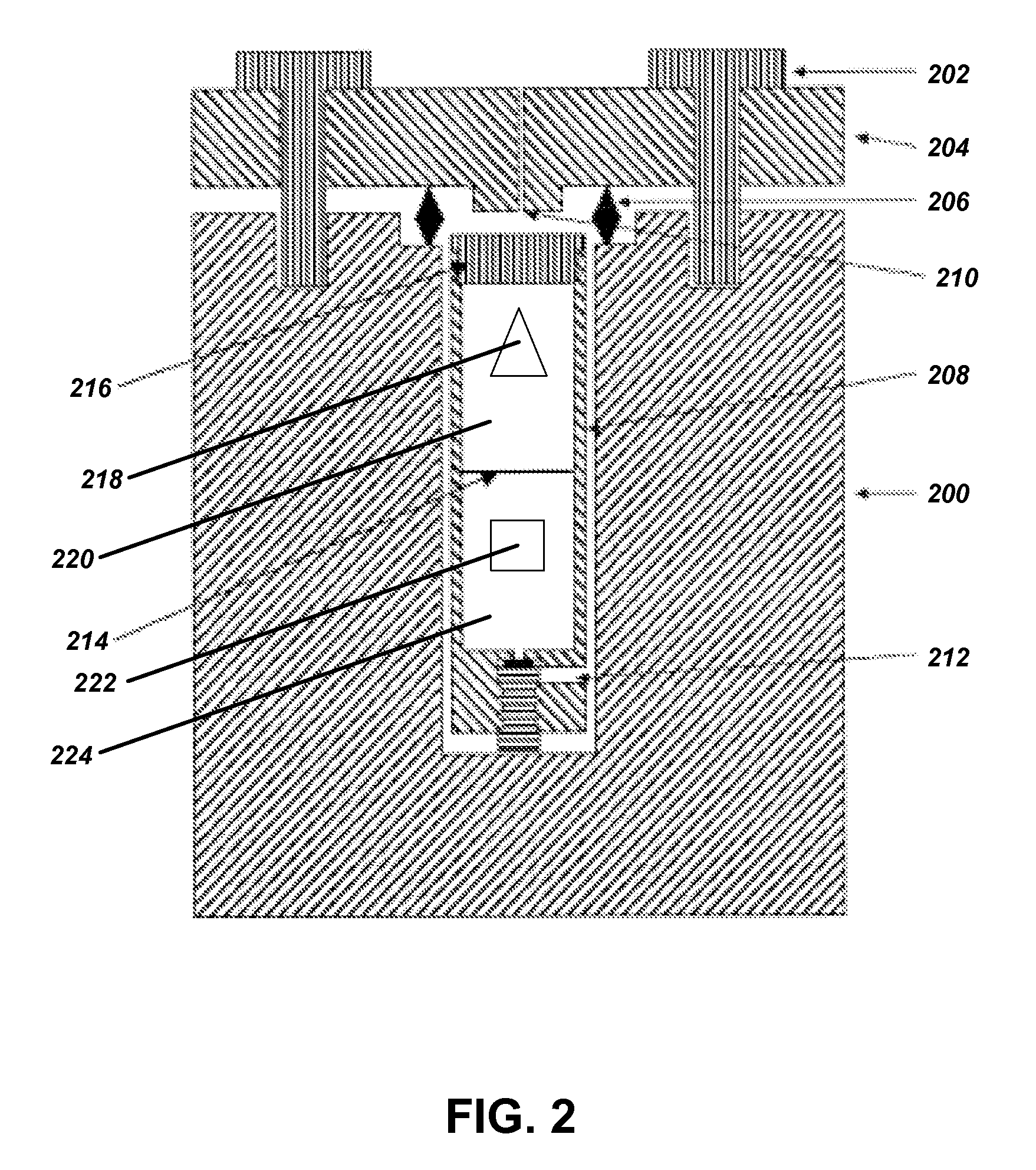
[0066] A large surface area, about 3 cm×4 cm, of a GaN seed crystal, a small surface area about 5 mm×5 mm, of some GaN seed crystals, 40 g of Ga metal, NaNH2 (1 mol % to ammonia), NaI (0.05 mol % to ammonia), 1.0 g of In metal, and 114.3 g of anhydrous liquid ammonia were loaded into the internal chamber. After transporting the internal chamber 208 into the autoclave 200 of which the inner diameter is about 5 cm, the autoclave 200 was heated at 625° C. (top region 220) and 675° C. (bottom region 224). The resulting maximum pressure was 31505 psi (2.2 kbar). The autoclave 200 was maintained at this high temperature for 1 day and the ammonia was released after 1 day. The resulting GaN crystal grown in the autoclave 200 according to the method of the present invention is shown in FIGS. 6(a) and 6(b). FIG. 6(a) shows the N-polar (N-face) surface and FIG. 6(b) shows the Ga-polar (Ga-face) surface. The thickne...

example 2

Growth of Smooth N-Polar (N-Face) GaN using Polycrystalline GaN in Ammonothermal Method

[0068] GaN seed crystals in size of about 5 mm×5 mm, about 120 g of polycrystalline GaN, NaNH2 (3 mol % to ammonia), and 101.3 g of anhydrous liquid ammonia were loaded into the internal chamber. After transporting the internal chamber 208 into the autoclave 200 of which the inner diameter is about 5 cm, the autoclave 200 was heated at 550° C. (top region 220) and 675° C. (bottom region 224). The resulting maximum pressure was 27686 psi (1.9 kbar). The autoclave 200 was maintained at this high temperature for 10 days and the ammonia was released after 10 days. About 2.5-2.6 microns of GaN films were grown on a seed crystal. Scanning electron microscope images of the resulting GaN crystal are shown in FIGS. 7(a) and 7(b). FIG. 7(a) shows the N-face and FIG. 7(b) shows the Ga-face. Similar to Example 1, the N-polar (N-face) surface was smoother than the Ga-polar (Ga-face). The N-face shown in FIG. ...

example 3

Growth of Smooth M-Plane GaN using Polycrystalline GaN in Ammonothermal Method

[0069] M-plane GaN seed crystals in size of about 3 mm×3 mm, about 100 g of polycrystalline GaN, NaNH2 (3.8 mol % to ammonia), and 101.5 g of anhydrous liquid ammonia were loaded into the internal chamber. After transporting the internal chamber 208 into the autoclave 200 of which the inner diameter is about 5 cm, the autoclave 200 was heated at 510° C. (top region 220) and 700° C. (bottom region 224). The resulting maximum pressure was 27986 psi (1.9 kbar). The autoclave 200 was maintained at this high temperature for 83 days and the ammonia was released after 83 days. Smooth M-plane GaN was grown on the M-plane GaN seed. FIG. 7C shows a photograph of the grown M-plane GaN.


PUM


Abstract

A method for growing III-V nitride films having an N-face or M-plane using an ammonothermal growth technique. The method comprises using an autoclave, heating the autoclave, and introducing ammonia into the autoclave to produce smooth N-face or M-plane Gallium Nitride films and bulk GaN.

Description

CROSS-REFERENCE TO RELATED APPLICATIONS [0001] The present application is related to the following application: [0002] U.S. Provisional Patent Application Ser. No. 60 / 790,310, filed Apr. 7, 2006, entitled “A METHOD FOR GROWING LARGE SURFACE AREA GALLIUM NITRIDE CRYSTALS IN SUPERCRITICAL AMMONIA AND LARGE SURFACE AREA GALLIUM NITRIDE CRYSTALS,” by Tadao Hashimoto, et al., Attorney Docket No. 30794.0179USP1; which application is incorporated by reference herein. [0003] This application claims the benefit under 35 U.S.C Section 119(e) of U.S. Provisional Application Ser. No. 60 / 815,507, filed on Jun. 21, 2006, by Tadao Hashimoto, Hitoshi Sato, and Shuji Nakamura, entitled “OPTO-ELECTRONIC AND ELECTRONIC DEVICES USING N-FACE GaN SUBSTRATE PREPARED WITH AMMONOTHERMAL GROWTH,” attorneys' docket number 30794.184-US-P1 (2006-666), which application is incorporated by reference herein.BACKGROUND OF THE INVENTION [0004] 1. Field of the Invention [0005] The invention is related to a method and...

Claims


Application Information

Patent Timeline
IPC IPC(8): H01L33/00C30B23/06H01L29/04H01L33/16
CPCC30B7/10C30B29/406H01L21/02389H01L21/02433H01L21/02458H01L21/0254Y10T117/1064H01L21/0262H01L29/045H01L29/2003H01L33/16Y10S438/973H01L21/02609
Inventor HASHIMOTO, TADAOSATO, HITOSHINAKAMURA, SHUJI
Owner SILVERBROOK RES PTY LTD
Why Eureka
Try Eureka