

Image sensor and fabrication method thereof
- Summary
- Abstract
- Description
- Claims
- Application Information
AI Technical Summary
Benefits of technology
Problems solved by technology
Method used
Image

Examples
Embodiment Construction
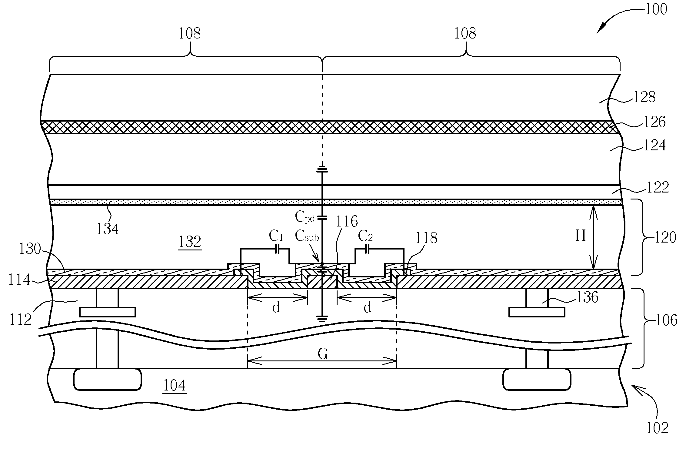
[0029]With reference to FIGS. 6-7, FIG. 6 is a sectional schematic diagram of an image sensor 100 according to the present invention, and FIG. 7 is a top view layout of a portion of the image sensor 100 shown in FIG. 6. The image sensor 100 is a photoconductor-on-active-pixel (POAP) image sensor, and is formed on a semiconductor chip 102 comprising a silicon substrate 104. The image sensor 100 comprises a dielectric layer 106 positioned on the substrate 104 and a plurality of pixels 108 defined on the substrate 104, wherein the pixels 108 are arranged as a pixel array 110, as shown in FIG. 7. Each pixel 108 comprises a pixel circuit 112 positioned in the dielectric layer 106, which may comprise at least a metal-oxide-semiconductor filed effect transistor (MOSFET), and a pixel electrode 114 of the pixel 108. The pixel electrodes 114 comprise metal materials, such as titanium nitride (TiN) and are electrically connected to the corresponding pixel circuits 112 vertically through the vi...
PUM
 Abstract
Description
Claims
Application Information