Electromagnetic Wave Detecting Element and Electromagnetic Wave Detection Device Using the Same

a technology of electromagnetic wave detection and electromagnetic wave, applied in the field of electromagnetic wave detection, can solve the problems of difficulty in deriving current transport property, uniform distribution, and difficulty in operation as a whole, and achieve the effects of simplifying the fabrication process, high sensitivity, and simplifying the devi

Inactive Publication Date: 2008-03-20
NAT INST OF INFORMATION & COMM TECH
View PDF3 Cites 4 Cited by
  • Summary
  • Abstract
  • Description
  • Claims
  • Application Information

AI Technical Summary

Benefits of technology

[0011] Owing to the fact that the same effect as mentioned above can be realized by using in the place of the normal conducting line a superconducting line that is made refined till the first superconducting electrode or the second superconducting electrode and the band structure thereof are varied this invention provides as the second aspect thereof an element comprising a plurality of structure units each comprising a flat substrate, a first superconducting electrode disposed on the substrate, a second superconducting electrode opposed to an upper part of the first superconducting electrode an insulating film not less than 5 nm and not more than 10 nm in thickness and sandwiched between the first and second superconducting electrodes, with parts of cross sections of the second superconducting electrode and insulating film formed on the upper part of the first superconducting electrode, and a superconducting line not more than 100 nm in width not more than 100 nm in thickness and passing just once through the cross sections of the second superconducting electrode and insulating film to form a sole weak link and establish electric connection of the first and second superconducting electrodes, wherein the first superconducting electrode of each of the structure units is serially connected to an adjacent second superconducting electrode the first or second superconducting electrodes of opposite end units are connected to leading lines, and the cross sections of the insulating films allowing passage of the superconducting lines are disposed so as to face a same direction with respect to the plurality of structure units laid throughout between the leading lines.
[0012] Another aspect of this invention resides in enabling the device and the process of fabrication to be simplified by having the first and second superconducting electrodes made of a same material.
[0013] Still another aspect of this invention resides in having the superconducting line and the first and second superconducting electrodes made of a same material. This is at an advantage in simplifying the device and the process of fabrication notwithstanding the superconducting line fated to constitute a weak link automatically acquires a varied material property because it is manufactured in a thin and narrow shape as described above.
[0014] Yet another aspect of this invention resides in causing the shortest length of the normal conducting line or the superconducting line required in connecting the first and second superconducting electrodes to become 0.3 to 6 times the superconducting coherent length. This is because this definition of the length is necessary for realizing conspicuous negative resistance from the current transport property due to the multiple-Andreev reflections in the two SN interfaces at the opposite ends of the N region.
[0015] Another aspect of this invention resides in giving the weak link a length in the range of 5 to 30 nm, a width in the range of 5 to 250 nm and a thickness in the range of 5 to 30 nm. The specified ranges are realistic conditions of process size allowing acquisition of the aforementioned effect as a mesoscopic SNS element and are necessary for the purpose of realizing a conspicuous negative resistance.
[0016] Still another aspect of this invention resides in allowing the first superconducting electrode and the second superconducting electrode to be formed in sizes included in a circle having a radius of not more than 5 times the wavelength of the electromagnetic wave to be detected. This restrictions in the manufacture of a detector of a prescribed surface areas is intended to enable the detector to over a large surface area with high sensitivity by giving the individual component elements a size small enough to perform detection with high sensitivity and causing these numerous component elements to be serially connected till they total the prescribed area. The SNS element is expected to manifest a veritably excellent performance as a detector for electromagnetic wave form millimeter-wave to X ray, γ ray and other high-energy particle rays. The criterions of the wavelength and the electrode size involved herein are decided by the fact that the energy of the electromagnetic wave subjected to detection belongs in the electromagnetic wave, infrared ray, ultraviolet light, X ray, γ ray and other high-energy particle rays having short wavelengths in excess of the energy gap of a superconductor and they are intended to prevent this energy from becoming unduly large as compared with the equivalent wavelength of the electromagnetic wave or the high-energy particle ray and resulting in degrading the resolution and the sensitivity. When the electromagnetic wave of a short wavelength having a larger energy than the energy gap of a superconductor is injected into the superconductor, excitation of numerous quasi-particles ensues. If the superconducting electrode is excessively large, the probability that the electromagnetic wave is inevitably relaxed before being detected as a change of conductance of the SNS element will grow and will result in degrading the sensitivity of detection. This is a dilemma between the increase of surface area and the increase of sensitivity of detection that confronts ordinary photoconductive detectors. In the case of the SNS element of series connection, the quasi-particle excitation that occurs at any part of the electrodes of the array of serially connected SNS junction elements is detected as a change of conductance of the whole serially connected elements. By selecting the electrode size and the number of series, it is rendered possible to realize an ultrahigh sensitivity detector having an arbitrary surface area. This detector is further endowed with such a high speed of response as several hundred GHz. In the far infrared to infrared regions, fully satisfactory detection of a single photon can be realized. Proper selection of the electrode size and the number of series enables realizing a detector befitting such elementary particles as neutrino, proton and neutron.

Problems solved by technology

Moreover, since the individual junctions suffer dispersion of resistance the potential distribution also becomes destitute of uniformity and the operation as a whole encounters difficulty in deriving the current transport property of the SNS aimed at.

Method used


Image

  • Electromagnetic Wave Detecting Element and Electromagnetic Wave Detection Device Using the Same
  • Electromagnetic Wave Detecting Element and Electromagnetic Wave Detection Device Using the Same
  • Electromagnetic Wave Detecting Element and Electromagnetic Wave Detection Device Using the Same

Examples


embodiment 1

[0037] An example of the process adopted for the formation of an electromagnetic wave detection element of this invention will be shown below.

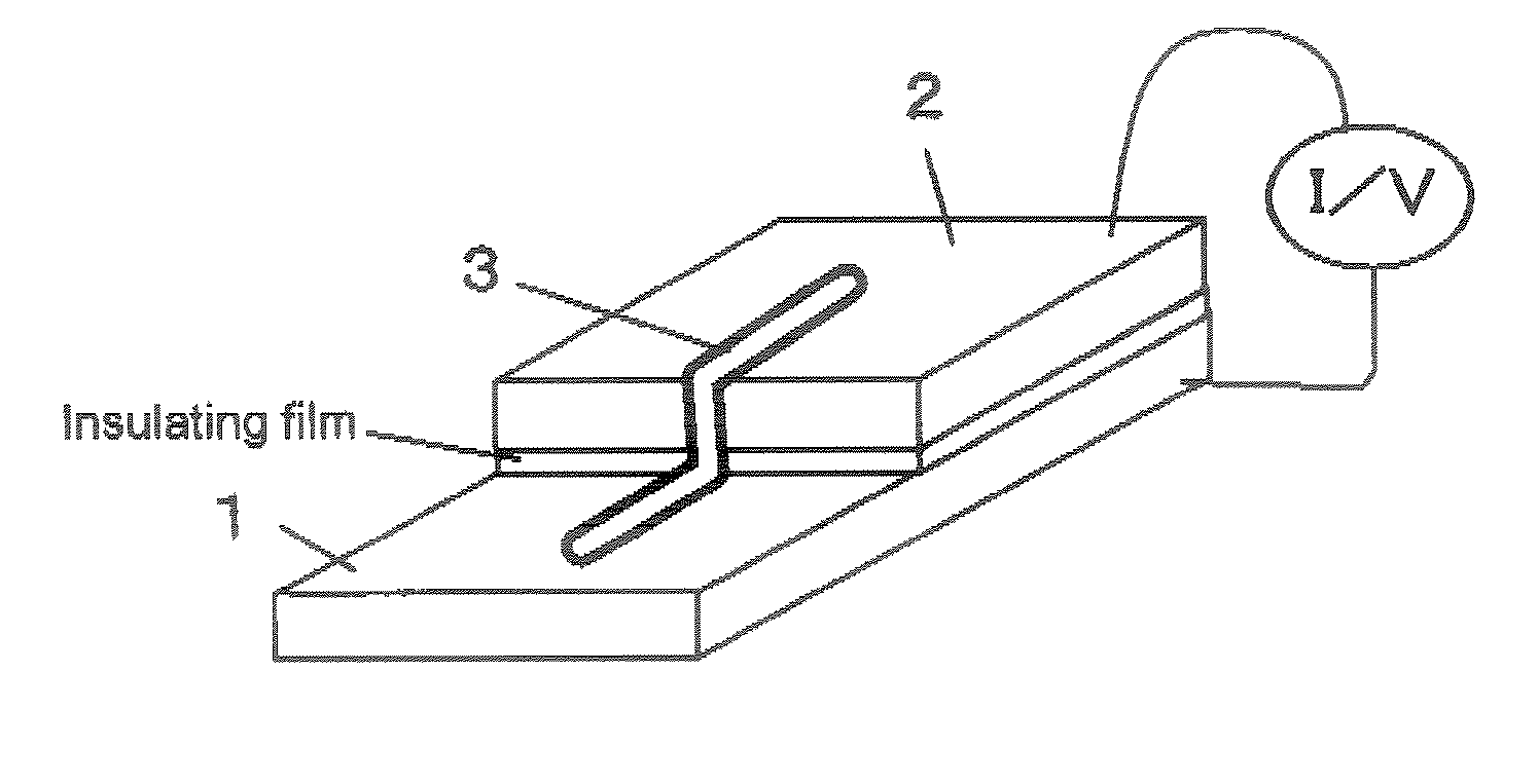
[0038] (1) On a substrate having an oxide film formed by thermal oxidation or deposition on the surface of a flat substrates such as a silicon substrate, films of a superconductor 1 made of niobium, niobium nitride, MgB2 or an oxide-based superconducting material are formed in a film thickness of 100 nm in an arrangement illustrated in FIG. 5 and are patterned by the ordinary lithography technique. This thickness nay vary in the range of 50 nm to 300 nm. Since the superconductor 1 is fated to become a first electrode during the patterning process, the size thereof prefers to be such that the upper limit thereof will be contained in a circle having a radius of not more than 5 times the wavelength of an electromagnetic wave to be detected and the lower limit of the whole size embracing electromagnetic waves and particle rays having a higher ene...

embodiment 2

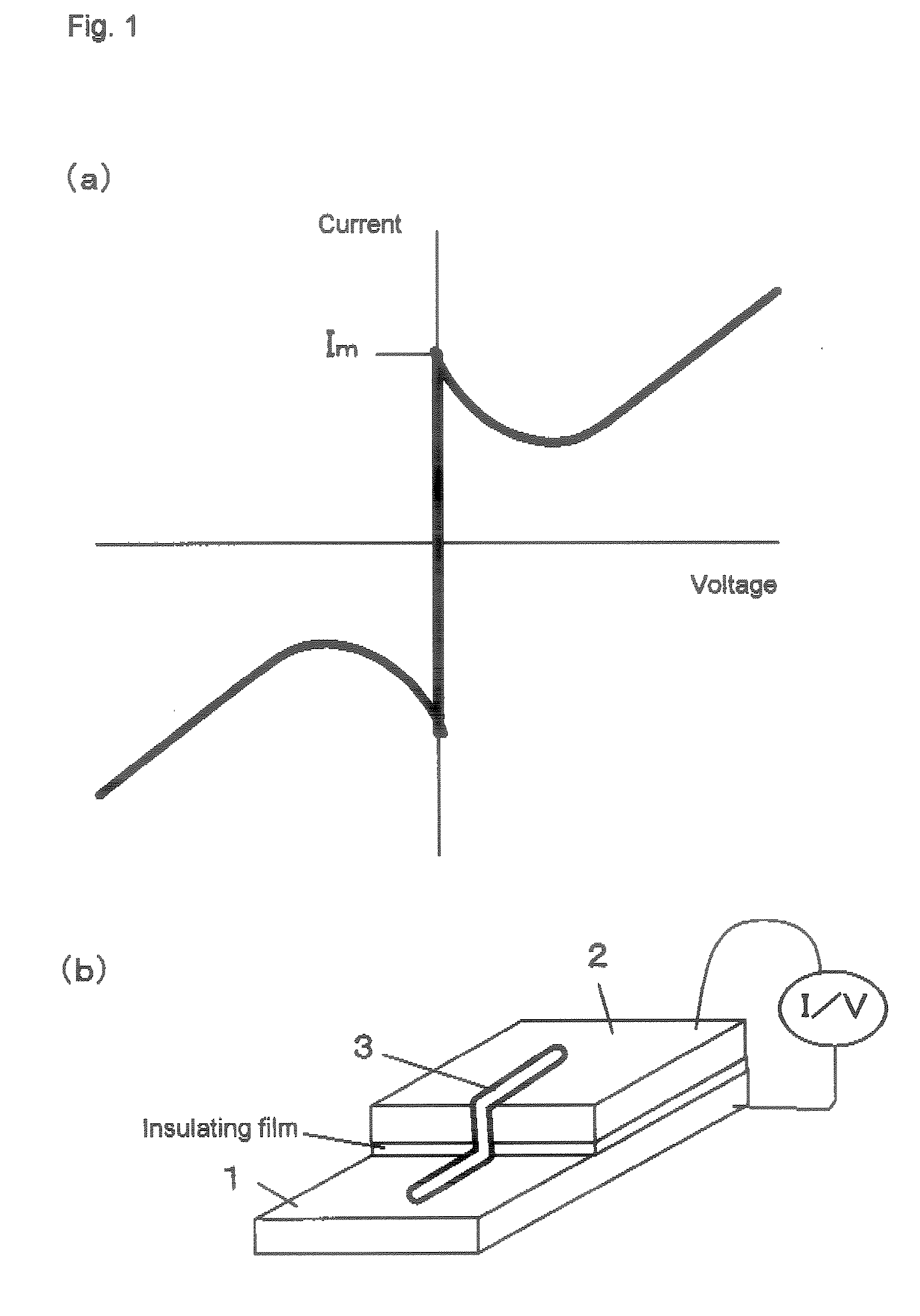
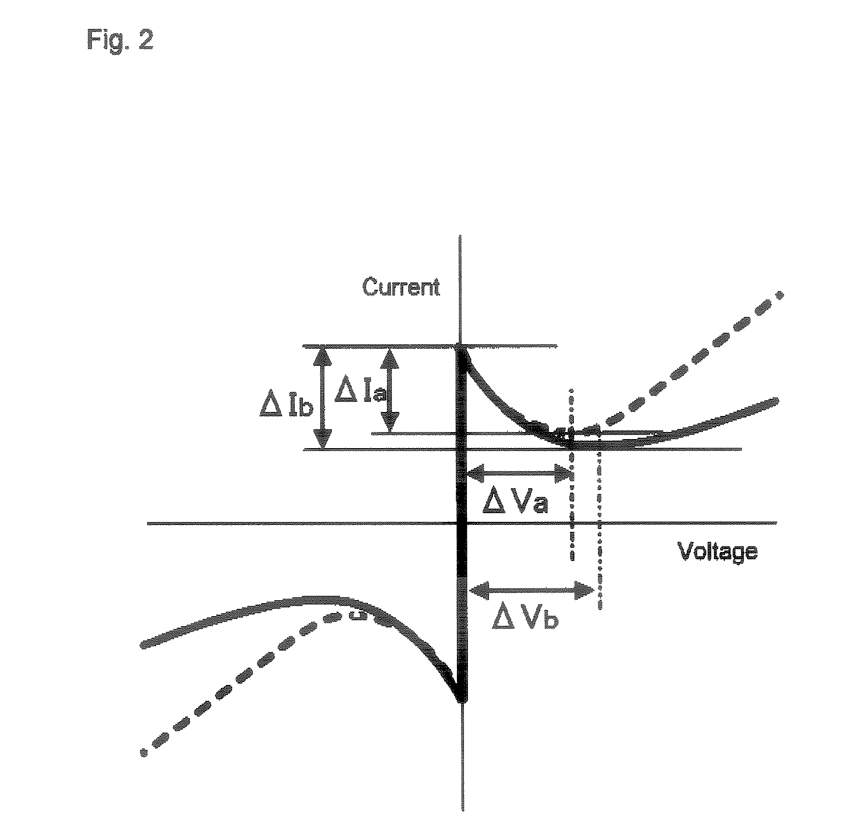
[0050]FIG. 8 illustrates the positions of bias voltage occurring during the detection of an electromagnetic wave by the use of an electromagnetic detection element 10. When the bias voltage is set at such positions of small voltage as approximates closely to zero in the negative resistance region as illustrated in the drawing, the electric current is varied with high sensitivity as indicated by the dotted line / solid line of FIG. 8 by the on / off of the radiation of the electromagnetic wave. By enabling the voltage bias condition dilated to not less than several times to be secured by the series connection, it is rendered possible to implement practical bias setting and accomplish detection of an electromagnetic wave with high sensitivity.

[0051] When the frequency of the electromagnetic wave subjected to detection exceeds the energy gap between the first and second superconducting electrodes, the electromagnetic wave detection element consequently obtained can be made to utilize effe...

embodiment 3

[0056]FIG. 9 is a block diagram depicting the case of configuring a detecting cell 20 using the electromagnetic detection elements 10. A bias voltage in the negative resistance region is applied as illustrated in FIG. 8 to the electromagnetic detection element 10 via a bias circuit 21 and the change in the electric current is detected by a sense amplifier 23 as transformed by a load 22 into a change in voltage. The output of the sense amplifier 23 is transmitted to a signal line via a switching circuit that is controlled with a signal for row address designation.

[0057] The structure that results from arraying the detecting cells 20 of FIG. 9 in the shape of a matrix is illustrated in FIG. 10. FIG. 10 represent a matrix of 3×3. It is evident that the structure of 3×1 enables implementing one-dimensional detection. It is also evident that the resolution during the course of detection can be enhanced by adding to the number of detecting cells 20 within a fixed surface area owing to th...


PUM


Abstract

It is possible to improve the negative resistance characteristic that can be expected when an SNS (superconductor-normal conductor-superconductor) structure is used as a structure unit for series connection. On the top of a first superconducting electrode, a second superconducting electrode is superimposed so as to sandwich an insulation film between the first and second superconducting electrodes, with parts of cross sections of the second superconducting electrode and insulation film placed on the top. A normal superconducting line electrically connects the first and second superconducting electrodes passing along the cross section of the insulation film, thereby constituting a structure unit having a single weak link. A plurality of such structure units connected in series are prepared. At the both ends of the series the first or second superconducting electrode is an element connected to a leading line. The structure units are arranged so that the cross sections of the insulation films along which the normal conducting line passes are arranged in the sale direction.

Description

TECHNICAL FIELD [0001] This invention relates to an electromagnetic wave detection element possessing an element structure i.e. SNS (superconductor-normal conductor-superconductor) or SS′S (superconductor-superconductor-superconductor) structure, which, when used as an amplifier, enables increasing the dynamic range of negative resistance as compared with the conventional equivalent and, when used as an electromagnetic wave detector, enables enhancing the detection sensitivity and to an electromagnetic wave detector apparatus using the element. BACKGROUND ART [0002] The current transport of the mesoscopic SNS junction, as described in T. Matsui and H. Ohta “Low-Voltage Negative Resistance Mixers of Nano-Meter SNS Junctions” (IEEE TRANSACTIONS ON APPLIED SUPERCONDUCTIVITY, VOL. 11, NO. 1, pp. 191-195, MARCH 2001) (hereinafter referred to as “Non-Patent Document 1”) or T. Matsui and H. Ohta. “Millimeter-and Submillimeter-Wave Negative Resistance SNS Mixers” (IEEE TRANSACTIONS ON APPLI...

Claims


Application Information

Patent Timeline
Patent Type & Authority Applications(United States)
IPC IPC(8): H01L29/06
CPCG01R29/0878H03D7/005H01L39/223H01L27/18Y10S505/702H10N69/00H10N60/12
Inventor MATSUIOHTA, HIROSHIKAWAKAMI, AKIRA
Owner NAT INST OF INFORMATION & COMM TECH
Why Eureka
Try Eureka