Euv Light Source, Euv Exposure Equipment, And Semiconductor Device Manufacturing Method

a technology of euv light source and exposure equipment, which is applied in the direction of optical radiation measurement, printers, therapy, etc., can solve the problems of insufficient resolution, limit the amount of plasma generated, and the density of plasma also becomes too high, so as to achieve good throughput and increase the production efficiency of semiconductor devices

Active Publication Date: 2008-03-20
NIKON CORP
View PDF12 Cites 7 Cited by
  • Summary
  • Abstract
  • Description
  • Claims
  • Application Information

AI Technical Summary

Benefits of technology

[0024] In this means, since an exposure apparatus with a good throughput is

Problems solved by technology

As the degree of integration of semiconductor integrated circuits has increased, circuit patterns have become finer, and the resolution has become insufficient in the case of conventionally used exposure apparatuses utilizing visible light or ultraviolet light.
However, in the case of techniques using Xe gas as a target, there are limits to how far a higher output EUV light source can be obtained, so that there is a demand for the use of other substances.
However, if Sn is used “as is” as a solid target, the density of the plasma that is generated also becomes too high, so that the exciting laser is absorbed by the generated plasma, or so that the EUV light itself that is generated from the plasma is also absorbed.
Accordingly, there is a problem in that the EUV light con

Method used


Image

  • Euv Light Source, Euv Exposure Equipment, And Semiconductor Device Manufacturing Method
  • Euv Light Source, Euv Exposure Equipment, And Semiconductor Device Manufacturing Method
  • Euv Light Source, Euv Exposure Equipment, And Semiconductor Device Manufacturing Method

Examples


Embodiment Construction

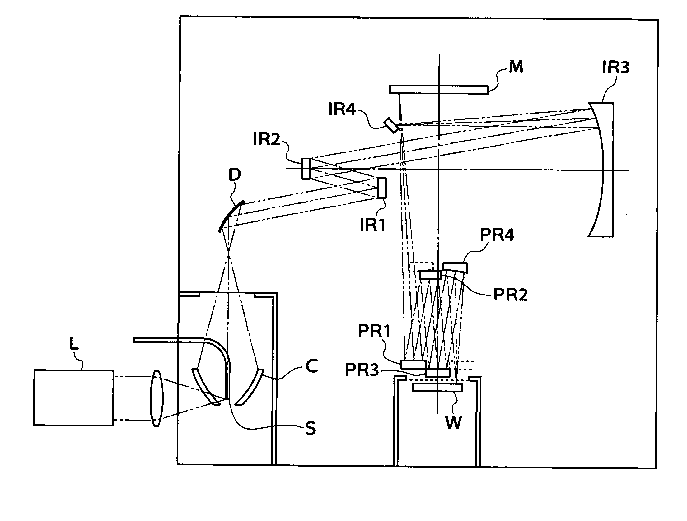
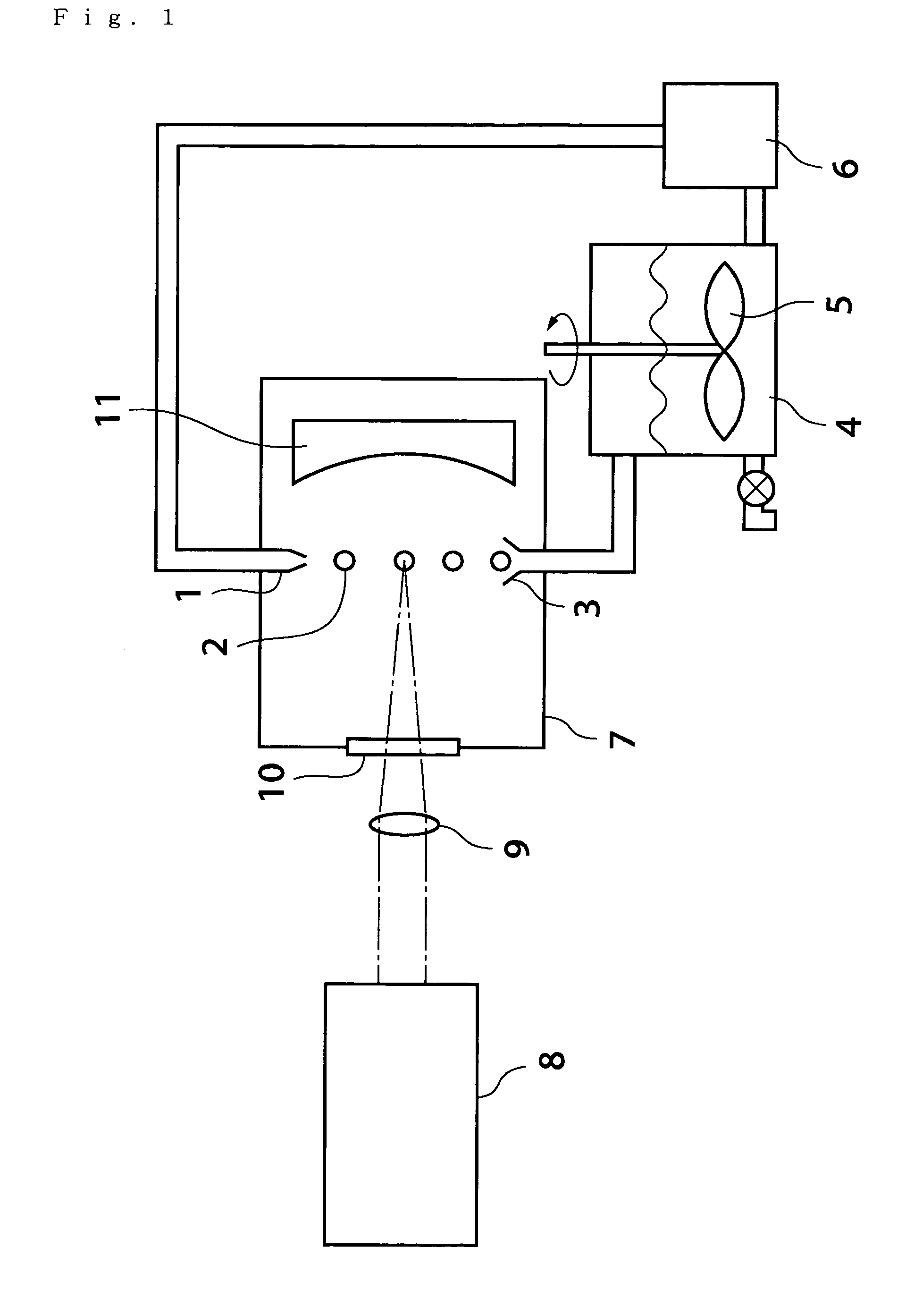
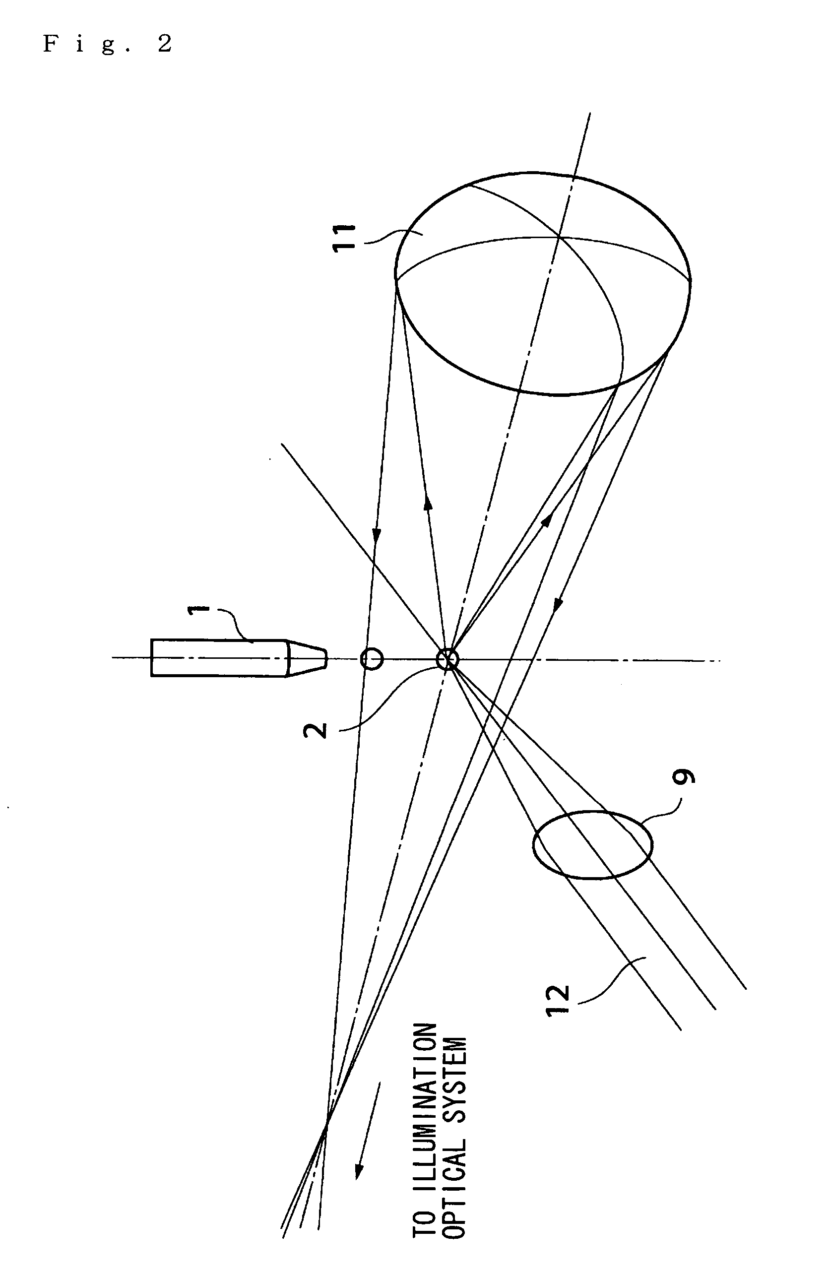
[0031] Working configurations of the present invention will be described below using the figures. FIG. 1 is a diagram showing an outline of a laser plasma EUV light source constituting a first working configuration of the present invention.

[0032] A liquid in which fine solid Sn particles are dispersed in a polystyrene resin is accommodated inside a heated tank 4. For example, the concentration of the fine solid Sn particles is 1 to 10 wt %. Furthermore, for example, the diameter of the fine solid Sn particles is 50 to 200 nm. A solution agitation mechanism 5 is provided in order to prevent the fine solid Sn particles from settling. In this example, the solution agitation mechanism 5 is a mechanism that causes vanes to rotate in the liquid.

[0033] The tank 4 is connected to a pressurizing pump 6 by piping, and the resin pressurized by this pressurizing pump is conducted to a nozzle 1, so that a liquid-form resin is caused to jet from the tip end of this nozzle 1 disposed inside a va...


PUM


Abstract

A liquid in which fine solid Sn particles are dispersed in a resin is accommodated inside the heated tank 4. The resin pressurized by a pressurizing pump is conducted to a nozzle 1, so that a liquid-form resin is caused to jet from the tip end of the nozzle 1 that is disposed inside a vacuum chamber 7. The liquid-form resin which is caused to jet from the nozzle 1 assumes a spherical shape as a result of surface tension, and is solidified by being cooled in a vacuum, so that a solid-form target 2 is formed. A laser introduction window 10 used for the introduction of laser light is formed in the vacuum chamber 7, and laser light generated from a laser light source 8 disposed on the outside of the vacuum chamber 7 is focused by a lens 9 and conducted into the vacuum chamber 7, so that the target is converted into a plasma, thus generating EUV light.

Description

TECHNICAL FIELD [0001] The present invention relates to an EUV light source which generates EUV light ((extreme ultraviolet light); in the present specification and patent claims, this refers to light having a wavelength of 100 nm or shorter), as well as an EUV exposure apparatus using this EUV light source, and a semiconductor device manufacturing method using this EUV exposure apparatus. BACKGROUND ART [0002] As the degree of integration of semiconductor integrated circuits has increased, circuit patterns have become finer, and the resolution has become insufficient in the case of conventionally used exposure apparatuses utilizing visible light or ultraviolet light. As is universally known, the resolution of an exposure apparatus is proportional to the numerical aperture (NA) of the transfer optical system, and is inversely proportional to the wavelength of the light that is used for exposure. Accordingly, as one means of increasing the resolution, there have been attempts to use ...

Claims


Application Information

Patent Timeline
IPC IPC(8): H05G2/00G03B27/54
CPCB82Y10/00G03F7/70033H05G2/005H05G2/003H05G2/008G21K2201/064G03F7/70008
Inventor MURAKAMI, KATSUHIKO
Owner NIKON CORP
Why Eureka
Try Eureka