Crystal producing apparatus, crystal producing method, substrate producing method, gallium nitride crystal, and gallium nitride substrate

a gallium nitride and crystal technology, applied in the direction of polycrystalline material growth, crystal growth process, chemically reactive gas, etc., can solve the problem of crystal defects (imperfections), the performance of devices such as light-emitting devices made from group-iii nitride semiconductors, and the difference between thermal expansion coefficients and lattice constants of substrates

Inactive Publication Date: 2008-04-03
RICOH KK
View PDF15 Cites 47 Cited by
  • Summary
  • Abstract
  • Description
  • Claims
  • Application Information

AI Technical Summary

Benefits of technology

[0013]It is an object of the present invention to at least partially solve the problems in the conventional technology.

Problems solved by technology

However, there is considerable difference between the coefficients of thermal expansion and the lattice constants of the substrate, which is made of sapphire or SiC, and the group-III nitride semiconductor.
Such differences in the physical properties of the substrate and the group-III nitride semiconductor result in causing crystal defects (imperfections) in the group-III nitride semiconductor.
If the group-III nitride semiconductor has crystal defects, performance of the device, such as a light-emitting device, made from the group-III nitride semiconductor degrades, e.g., device lifetime is shortened, large driving power is necessary, and the like.
However, because sapphire is insulating, it is difficult to obtain an electrode from such an insulating substrate, requiring obtaining an electrode from a group-III nitride semiconductor.
To obtain an electrode from a group-III nitride semiconductor, a device needs to be large, resulting in increasing necessary costs.
Furthermore, if the device size increases, the substrate may warp because of the differences in the physical properties of the sapphire substrate and the group-III nitride semiconductor.
In a group-III nitride semiconductor device formed on a sapphire substrate, separation of chips by use of cleavages is difficult, so that it is difficult to obtain a desired resonator facet for a laser diode (LD).
In this approach, however, it is difficult to form a resonator facet and to conduct chip separation in a single process, unlike a process for forming a conventional LD.
As a result, manufacturing costs increase due to necessity of extra processes.
Although occurrence of crystal defect can be reduced in this approach, it is still difficult to solve problems related to insulation properties or cleavage of a sapphire substrate.
Therefore, it is difficult to obtain desired flatness on a surface of a GaN crystal, resulting in making it difficult to produce a bulked GaN crystal in desired quality with less defect density.
Furthermore, when a GaN crystal is polished and sliced, mechanical damage and etching easily occurs in a crystal grain boundary or a region of dislocation.
Thus, it is difficult to produce a wafer in desired quality with preferable flatness of its surface.

Method used


Image

  • Crystal producing apparatus, crystal producing method, substrate producing method, gallium nitride crystal, and gallium nitride substrate
  • Crystal producing apparatus, crystal producing method, substrate producing method, gallium nitride crystal, and gallium nitride substrate
  • Crystal producing apparatus, crystal producing method, substrate producing method, gallium nitride crystal, and gallium nitride substrate

Examples


Embodiment Construction

[0042]Exemplary embodiments of the present invention are explained in detail below with reference to the accompanying drawings. Same reference numerals are assigned to the same or substantially the same units, members, portions, and the like, and explanations thereof are omitted.

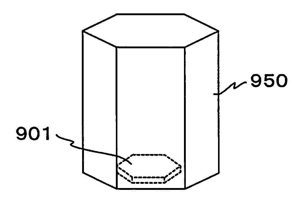
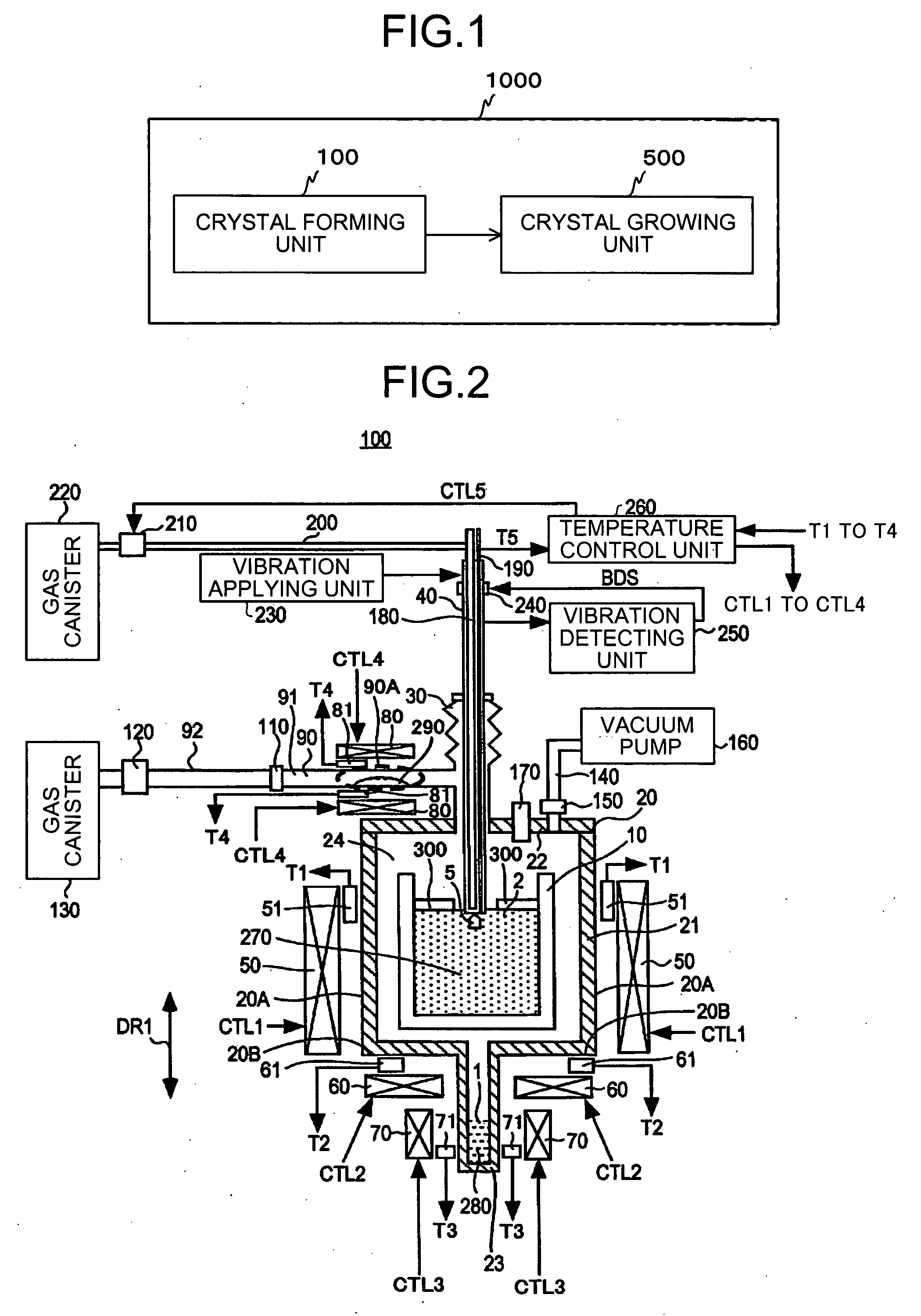
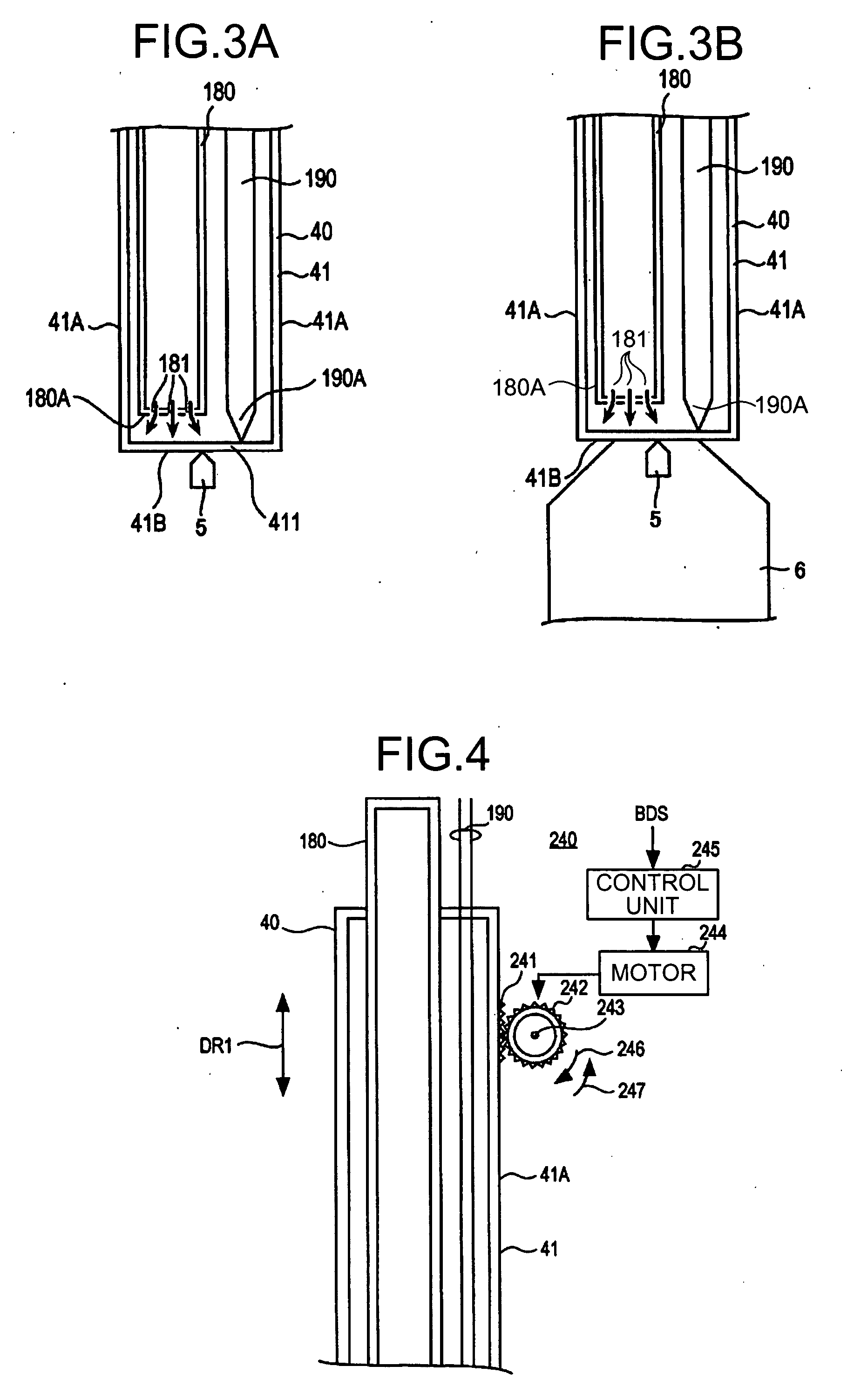
[0043]FIG. 1 is a schematic diagram of a crystal producing apparatus 1000 that produces a bulked gallium nitride (GaN) crystal according to an embodiment of the present invention. The crystal producing apparatus 1000 includes a crystal forming unit 100 and a crystal growing unit 500. The crystal forming unit 100 forms a GaN crystal by supplying nitride gas into melt mixture containing metal sodium (Na) and metal gallium (Ga). In other words, the crystal forming unit 100 forms a GaN crystal by the flux method. A GaN crystal formed by the crystal forming unit 100 will be called “a first GaN crystal” for convenience of explanation.

[0044]The crystal growing unit 500 grows a GaN crystal on the first GaN crystal b...


PUM

PropertyMeasurementUnit
thickaaaaaaaaaa
temperatureaaaaaaaaaa

Abstract

A crystal producing apparatus includes a crystal forming unit and a crystal growing unit. The crystal forming unit forms a first gallium nitride (GaN) crystal by supplying nitride gas into melt mixture containing metal sodium (Na) and metal gallium (Ga). The first GaN crystal is sliced and polished to form GaN wafers. The crystal growing unit grows a second GaN crystal on a substrate formed by using a GaN wafer, by the hydride vapor phase epitaxy method, thus producing a bulked GaN crystal.

Description

CROSS-REFERENCE TO RELATED APPLICATIONS[0001]The present application claims priority to and incorporates by reference the entire contents of Japanese priority documents, 2006-270363 filed in Japan on Oct. 2, 2006 and 2007-198607 filed in Japan on Jul. 31, 2007.BACKGROUND OF THE INVENTION[0002]1. Field of the Invention[0003]The present invention relates to a technology for producing a gallium nitride (GaN) crystal and a GaN substrate.[0004]2. Description of the Related Art[0005]Indium gallium aluminum (InGaAln)-based devices (group-III nitride semiconductor) are popularly used as ultraviolet light sources, purple light sources, blue light sources, or green light sources. Such group-III nitride semiconductor devices are typically formed on a substrate made of sapphire or silicon carbide (SiC) by metalorganic chemical vapor deposition (MOCVD) method or molecular beam epitaxy (MBE) method.[0006]However, there is considerable difference between the coefficients of thermal expansion and t...

Claims


Application Information

Patent Timeline
Patent Type & Authority Applications(United States)
IPC IPC(8): C01B21/06C30B25/02H01L21/20H01L33/32
CPCC30B9/12C30B17/00C30B23/025C30B25/20Y10T117/10C30B9/00C30B25/18H01L21/20H01L29/2003C30B29/403
Inventor SARAYAMA, SEIJIIWATA, HIROKAZU
Owner RICOH KK
Why Eureka
Try Eureka