Semiconductor device and method for manufacturing same

a semiconductor device and semiconductor technology, applied in the direction of semiconductor devices, electrical devices, transistors, etc., can solve the problems of difficult to satisfy all, problematically deteriorating planarity of the top surface of the gate electrode, etc., to improve the characteristics of the semiconductor device, improve the flexibility of selection of conductive materials, and optimize the manufacturing process

Active Publication Date: 2008-04-17
SONY CORP
View PDF3 Cites 68 Cited by
  • Summary
  • Abstract
  • Description
  • Claims
  • Application Information

AI Technical Summary

Benefits of technology

[0057]As the base including the source / drain regions, the channel forming regions and so on used in the present invention, besides a semiconductor substrate, a support member of which surface has a semiconductor layer (e.g., a glass substrate, quartz substrate, silicon substrate of which surface has an insulating layer, plastic substrate, or plastic film) can be used. The insulated gate field effect transistor is formed in e.g. a well region or the like in a semiconductor substrate or semiconductor layer. A so-called element isolation region having e.g. a trench structure may be formed between the insulated gate field effect transistors. The element isolation region may have a LOCOS structure, or may be based on the combination of a trench structure and LOCOS structure. More alternatively, the base having an SOI structure arising from SIMOX or substrate bonding may be used. In this case, the formation of the element isolation region is unnecessary.
[0058]In the semiconductor device and the method for manufacturing the same according to the first embodiment of the present invention, in the formation of the contact plug formation openings in the interlayer insulating layer through a series of etching processes, the protective layers formed on the top surfaces of the gate electrodes are exposed at the bottoms of the contact plug formation openings in which the gate electrode contact plugs are to be formed. Therefore, in any of the case in which the top surface of the NMISFET gate electrode and the top surface of the PMISFET gate electrode are composed of different conductive materials, the case in which the top surface of the NMISFET gate electrode is composed of plural conductive materials different from each other, and the case in which the top surface of the PMISFET gate electrode is composed of plural conductive materials different from each other, the differences in the etching selection ratio and so on among these conductive materials lead to no problem. Thus, the semiconductor device and the method for manufacturing the same according to the first embodiment of the present invention enhance the flexibility of selection of conductive materials of the gate electrodes to thereby allow improvement in characteristics of the semiconductor device and optimization of the manufacturing process.
[0059]In the semiconductor device and the method for manufacturing the same according to the second embodiment of the present invention, the interconnect layers are formed to cover the top surfaces of the respective gate electrodes of the N-channel insulated gate field effect transistor and the P-channel insulated gate field effect transistor. Therefore, each of the gate electrodes can be formed by using a conductive material having a favorable work function value. In addition, because the interconnect layers are provided, increase in the electric resistance hardly occurs as a whole even when the gate length becomes smaller. Moreover, if contact plugs are provided above the interconnect layers, in the formation of the contact plug formation openings in the interlayer insulating layer through a series of etching processes, the interconnect layers are exposed at the bottoms of the contact plug formation openings in which the gate electrode contact plugs are to be formed. Therefore, although the top surface of the NMISFET gate electrode and the top surface of the PMISFET gate electrode are composed of different conductive materials, the differences in the etching selection ratio and so on between these conductive materials lead to no problem. Thus, the semiconductor device and the method for manufacturing the same according to the second embodiment of the present invention enhance the flexibility of selection of conductive materials of the gate electrodes to thereby allow improvement in characteristics of the semiconductor device and optimization of the manufacturing process.

Problems solved by technology

However, when in a semiconductor device including different kinds of insulated gate field effect transistors, such as a CMOS semiconductor device or BiCMOS semiconductor device including an NMOS and PMOS, the gate electrodes of the NMOS and the PMOS are formed by using different conductive materials, it is difficult to satisfy all of the following conditions: each of the gate electrodes has a favorable work function value; the material of each of the gate electrodes provides a sufficiently high etching selection ratio; and the material of each of the gate electrodes has sufficient resistance against chemical treatment performed after the etching.
This difficulty will act as a factor in inhibition of optimization of the fabrication process for the semiconductor device.
Thus, for example, due to the difference in the etching selection ratio between these conductive materials, the planarity of the top surface of the gate electrode will be problematically deteriorated when the top surface is subjected to etching treatment.

Method used


Image

  • Semiconductor device and method for manufacturing same
  • Semiconductor device and method for manufacturing same
  • Semiconductor device and method for manufacturing same

Examples


first embodiment

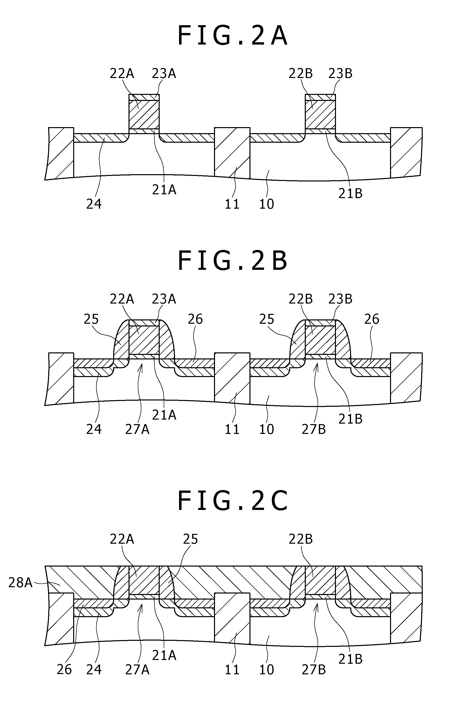
[0075]A first embodiment of the present invention relates to a semiconductor device and a method for manufacturing the same according to the first embodiment of the present invention. Insulated gate field effect transistors included in the semiconductor device of the first embodiment are MOSFETs. Furthermore, the semiconductor device of the first embodiment includes an NMOS and PMOS. This is the same also in other embodiments to be described later.

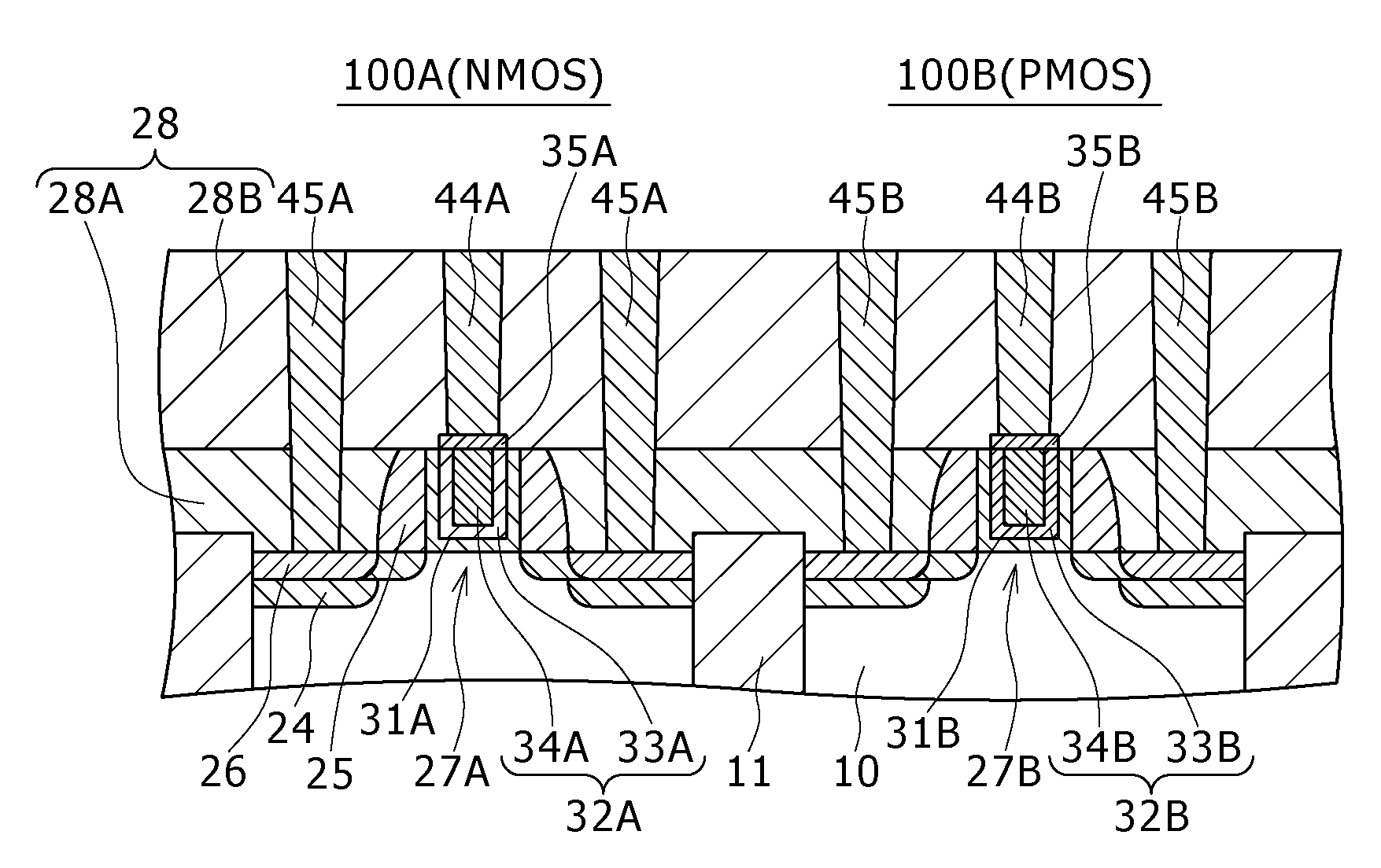
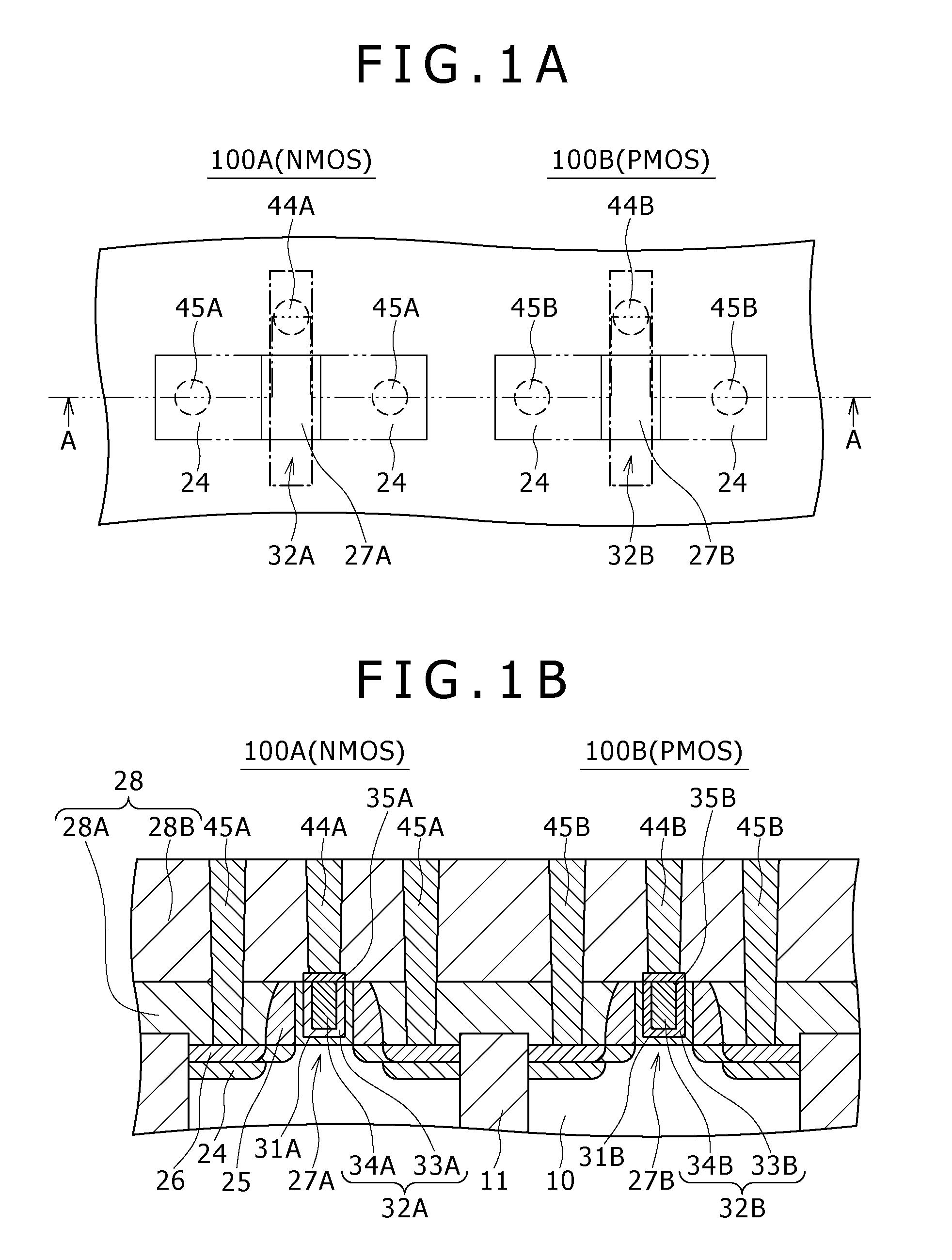
[0076]FIG. 1A schematically shows a projected image of an NMOS 100A and a PMOS 100B included in the semiconductor device of the first embodiment. In FIG. 1(A), the dashed line represents various kinds of contact plugs, the one-dot chain line represents gate electrodes, and the two-dot chain line represents source / drain regions and channel forming regions. FIG. 1B is a partial sectional view along the three-dot chain line indicated by arrowheads A in FIG. 1A.

[0077]The semiconductor device of the first embodiment includes the NMOS 100A as an...

second embodiment

[0105]A second embodiment of the present invention is a modification of the first embodiment. A projected image of an NMOS 200A and a PMOS 200B included in a semiconductor device of the second embodiment is the same as that of FIG. 1A. FIG. 3 is a partial sectional view of the semiconductor device of the second embodiment, equivalent to the partial sectional view along the three-dot chain line indicated by arrowheads A in FIG. 1A. Components of the NMOS 200A and the PMOS 200B are basically the same as those in the first embodiment, and hence are given the same reference numerals as those in the first embodiment. This is the same also in other embodiments to be described later.

[0106]The second embodiment is different from the first embodiment in that a gate electrode 32A of the NMOS 200A has a multilayer structure formed of conductive material layers 33A, 33B, and 34A. With reference to FIGS. 4A to 4C, a method for manufacturing the semiconductor device of the second embodiment will ...

third embodiment

[0115]A third embodiment of the present invention is also a modification of the first embodiment. A projected image of an NMOS 300A and a PMOS 300B included in a semiconductor device of the third embodiment is the same as that of FIG. 1A. FIG. 5 is a partial sectional view of the semiconductor device of the third embodiment, equivalent to the partial sectional view along the three-dot chain line indicated by arrowheads A in FIG. 1A.

[0116]The third embodiment is different from the first embodiment mainly in that formation of a third conductive material layer 34 is omitted. With reference to FIGS. 6A and 6B, a method for manufacturing the semiconductor device of the third embodiment will be described below.

[Step-300]

[0117]Initially, based on steps similar to [Step-100] and [Step-110] of the first embodiment, a semiconductor substrate 10 (base) is obtained that is composed of silicon (Si) and includes channel forming regions 27A and 27B of the NMOS 300A and the PMOS 300B, source / drain ...


PUM


Abstract

Disclosed herein is a semiconductor device including an N-channel insulated gate field effect transistor and a P-channel insulated gate field effect transistor, the device having: a first insulating layer and a second insulating layer; and gate electrode contact plugs. Each of the gate electrodes of the N-channel insulated gate field effect transistor and the P-channel insulated gate field effect transistor is buried in a gate electrode formation opening provided in the first insulating layer.

Description

CROSS REFERENCES TO RELATED APPLICATIONS[0001]The present invention contains subject matter related to Japanese Patent Application JP 2006-281026 filed with the Japan Patent Office on Oct. 16, 2006 and Japanese Patent Application JP 2007-161030 filed with the Japan Patent Office on Jun. 19, 2007, the entire contents of which being incorporated herein by reference.BACKGROUND OF THE INVENTION[0002]1. Field of the Invention[0003]The present invention relates to a semiconductor device including an N-channel insulated gate field effect transistor and a P-channel insulated gate field effect transistor, and a method for manufacturing the same.[0004]2. Description of the Related Art[0005]For an insulated gate field effect transistor (metal insulator semiconductor FET (MISFET)) such as a MOSFET, the combination of a gate insulating film composed of silicon oxide and a gate electrode formed of a polycrystalline silicon film is widely used. For example, in a CMOS semiconductor device, there is...

Claims


Application Information

Patent Timeline
Patent Type & Authority Applications(United States)
IPC IPC(8): H01L27/092H01L21/8238
CPCH01L21/823842H01L29/66545H01L21/823871H01L21/76895
Inventor TAI, KAORITSUKAMOTO, MASANORINAKATA, MASASHIOSHIYAMA, ITARU
Owner SONY CORP
Why Eureka
Try Eureka