

Semiconductor Wafer And Semiconductor Device
a semiconductor and semiconductor technology, applied in the field of semiconductor devices, can solve problems such as peeling, safety and handling problems, shortening the process, etc., and achieve the effect of excellent low stress properties and adhesion, and low residual stress
- Summary
- Abstract
- Description
- Claims
- Application Information
AI Technical Summary
Benefits of technology
Problems solved by technology
Method used
Image

Examples
example 1
[0062] This example illustrates a copolymer (A-1) of 5-decyl-2-norbornene (hereinafter, referred to as “decyl norbornene”) / 5-[(2,3-epoxypropoxy)methyl]-2-norbornene (hereinafter, referred to as “glycidyl methyl ether norbornene”)=70 / 30.
[0063] All glassware was dried at 60° C. under a 0.1 torr vacuum for 18 hours. The glassware was then transferred into a glovebox and attached thereto. After ethyl acetate (917 g), cyclohexane (917 g), decyl norbornene (192 g, 0.82 mol), and glycidyl methyl ether norbornene (62 g, 0.35 mol) were added into a reaction flask, the reaction flask was taken out from the glovebox, and dry nitrogen gas was introduced into the reaction flask.
[0064] The reaction medium was degassed by passing a stream of nitrogen gas through the solution for 30 minutes. Inside the glovebox, a nickel catalyst, i.e., bis(toluene)bis(perfluorophenyl) nickel (9.36 g, 19.5 mmol), was dissolved in 15 ml of toluene, and taken up in a 25 mL syringe. The syringe was taken out from th...
example 2
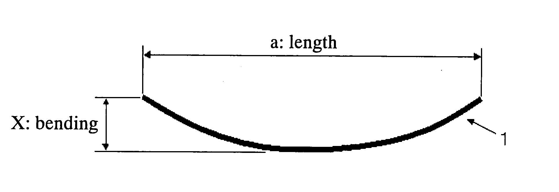
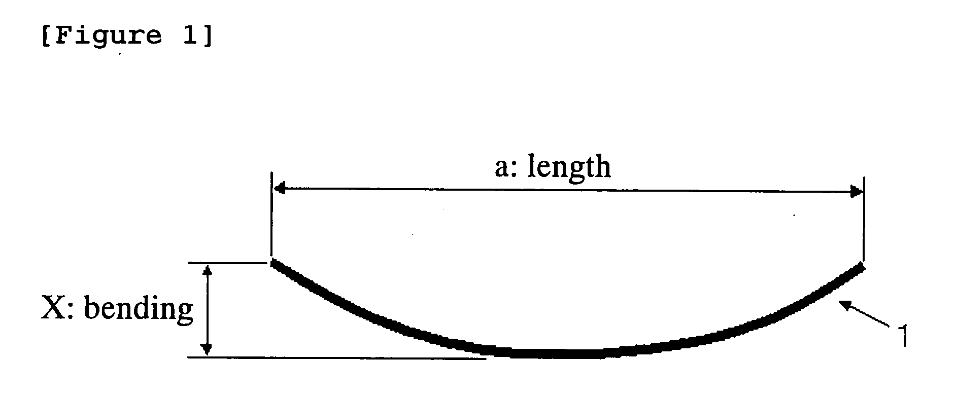
[0081] The backside of the wafer produced in the same manner as in Example 1 and having a thickness of 725 μm was ground to 200 μm. However, breaking and cracking or the like did not occur, and a thin wafer was obtained. Then, the bending of this wafer measured by the surface roughness meter was 370 μm. The stress calculated was 5 MPa.
example 3
[0082] A terpolymer (A-2) of decyl norbornene / glycidyl methyl ether norbornene / phenethyl norbornene=55 / 30 / 15 was obtained in the same manner as in Example 1 except that decyl norbornene (129 g, 0.55 mol) and glycidyl methyl ether norbornene (177 g, 0.30 mol) and 5-(2-phenylethyl)-2-norbornene (hereinafter, referred to as “phenethyl norbornene”) (29.7 g, 0.15 mol) were used in place of decyl norbornene (192 g, 0.82 mol) and glycidyl methyl ether norbornene (62 g, 0.35 mol) of Example 1. The polymerization and the reprecipitation were carried out, and 309 g (yield: 92%) of a polymer after drying was collected. The polymer obtained had a molecular weight by GPC Mw=30000, Mn=68000, Mw / Mn=2.3. Polymer composition by H-NMR 54 mole % decyl norbornene; 31 mole % glycidyl methyl ether norbornene; and 15 mole % phenethyl norbornene.
[0083] Evaluation was made in the same manner as in Example 1.
[0084] The solder reflow resistance test and the operation confirmation of the semiconductor device...
PUM
| Property | Measurement | Unit |
|---|---|---|
| thickness | aaaaa | aaaaa |
| thickness | aaaaa | aaaaa |
| thickness | aaaaa | aaaaa |
Abstract
Description
Claims
Application Information