

Nanometer-scale sharpening of conductor tips
a technology of conductor tips and nanometers, which is applied in the direction of instruments, scanning probe techniques, vacuum evaporation coating, etc., can solve the problems of avoiding the need for careful monitoring of the process and the need for expensive monitoring devices, and achieves the effect of increasing production throughpu
- Summary
- Abstract
- Description
- Claims
- Application Information
AI Technical Summary
Benefits of technology
Problems solved by technology
Method used
Image

Examples
example 1
Simulation of Beam-Tip Interaction for Perfectly Conductive Materials
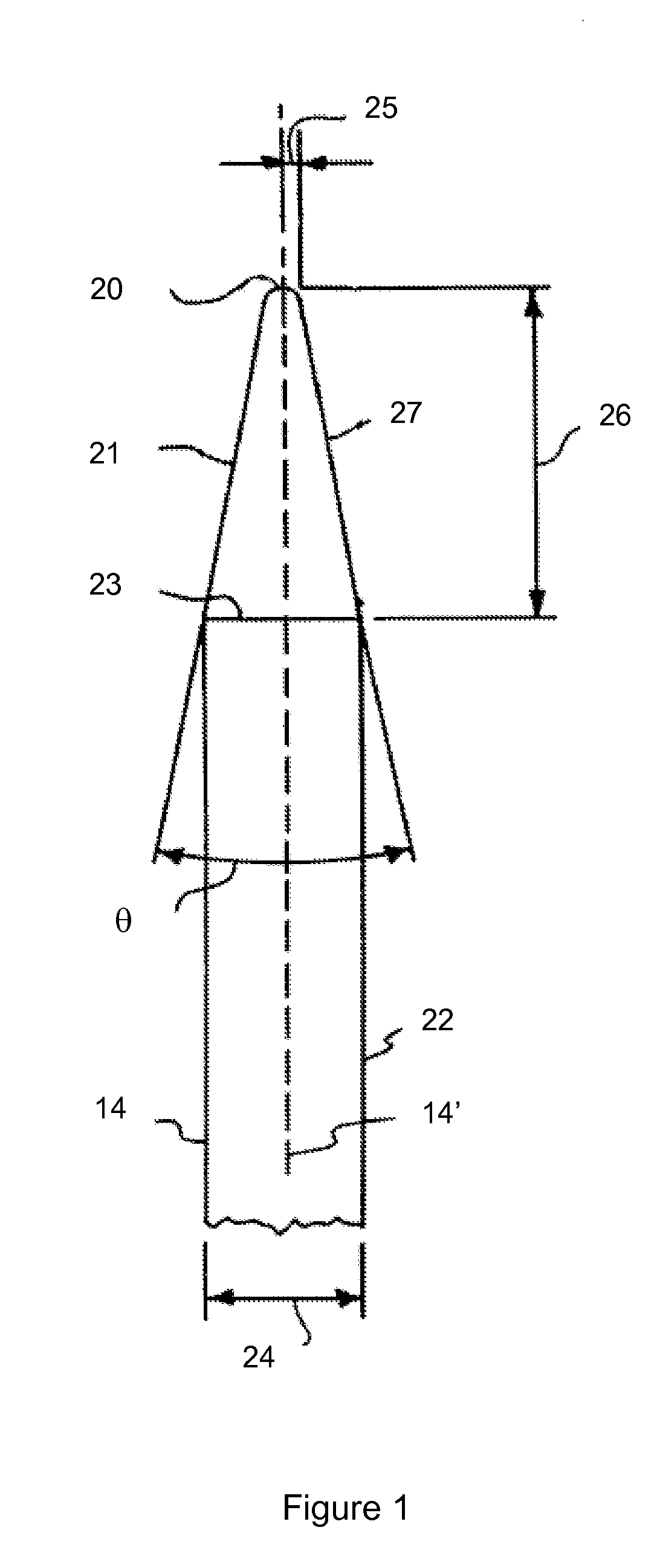
[0083]The electric field surrounding a biased conductor with a sharp tip was simulated for a two-dimensional case assuming that the material was a perfect conductor, resulting in an absence of electric fields within the tip. The electric potential was also assumed to be constant and present across the entirety of the conductor. The simulations demonstrated that the electric field was dramatically enhanced near the apex of the tip. The sharper the tip, the more prominent the enhancement.
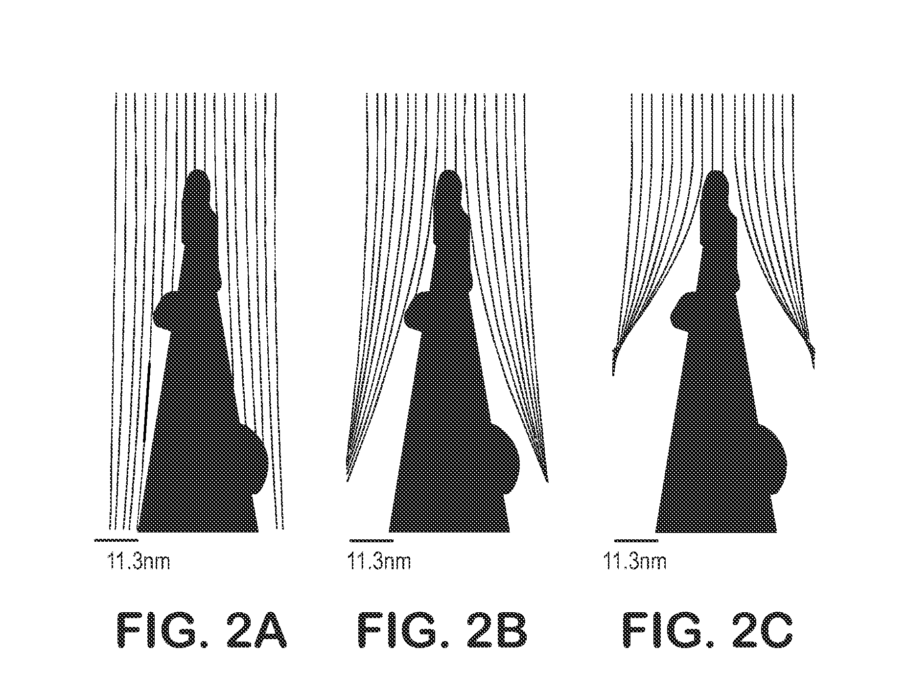
[0084]The ion motion surrounding the biased conductor tip was also simulated. FIGS. 2A, 2B, and 2C present ion path simulation results for a neon ion beam aligned with the longitudinal axis of the conductor. The ion beam accelerating voltage was 2000 eV; the neon atoms were singly ionized. FIGS. 2A, 2B, and 2C show simulation results for tip potentials of 100 V, 400V, and 800 V respectively. As anticipated, the charged particles are ...
example 2
Sharpening of Pt—Ir Tips
[0086]The experimental setup consisted of a vacuum chamber with a background pressure of approximately 5×10⁻⁹ torr, which is attached to an ultra-high vacuum system containing a scanning tunneling microscope. Within the vacuum chamber was a Model 04-161 ion gun from Physical Electronics (advertised current density 300 μA / cm2) controlled by a Model IPS Ion Sputtering Gun Power Supply from OCI Vacuum Microengineering, and a micromanipulator with x, y, z and rotational adjustments. Tip bias was provided by a Model M107 DC Voltage Source from Systron-Donner. Transmission electron microscope (TEM) imaging of the tips ex-situ was performed with a Philips CM200 microscope.
[0087]Platinum-iridium scanning tunneling microscopy probes were purchased commercially from Material Analytical Services (MAS). The initial apex radius of curvature of the Pt—Ir tips was roughly 100 nm.
[0088]FIGS. 5A through 5F show TEM images of a Pt—Ir tip prior to sputtering (FIG. 5A) and at va...
example 3
Sharpening of Tungsten Tips
[0091]The sputtering apparatus was as described in Example 2.
[0092]Tungsten wires with electrochemically etched tips were prepared by etching polycrystalline tungsten wire in sodium hydroxide solution. The initial apex radius of curvature of the tungsten tips was roughly 100 nm.
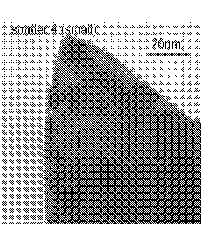
[0093]FIG. 6A shows a TEM image of a W tip prior to sputtering; a large flat face is present at the tip apex. FIG. 6B shows a TEM image of a W tip after sputtering; the tip radius is approximately 1.5 nm, time approx 15 min. The tip voltage was 400 V and the neon ion energy was 2000 eV. The ion beam was directed substantially parallel to the longitudinal axis of the tip. The scale marker in FIG. 6A is 50 nm; that in FIG. 6B is 20 nm.
[0094]For a control experiment with zero tip bias and 2000 eV beam accelerating voltage the resulting tip radius was approximately 6 nm.
PUM
| Property | Measurement | Unit |
|---|---|---|
| Length | aaaaa | aaaaa |
| Radius | aaaaa | aaaaa |
| Electric potential / voltage | aaaaa | aaaaa |
Abstract
Description
Claims
Application Information