Thin wafer detectors with improved radiation damage and crosstalk characteristics

a detector and thin wafer technology, applied in the field of thin wafer detectors, can solve the problems of affecting the performance of detectors, transistors and integrated circuits, affecting the width of the depletion region, and increasing reverse bias current and forward voltage, so as to reduce radiation damage susceptibility, reduce crosstalk, and reduce the effect of dark curren

Active Publication Date: 2008-06-05
OSI OPTOELECTRONICS
View PDF73 Cites 102 Cited by
  • Summary
  • Abstract
  • Description
  • Claims
  • Application Information

AI Technical Summary

Benefits of technology

[0018]The present invention is directed toward a detector structure, detector arrays, and a method of detecting incident radiation. The present invention comprises several embod

Problems solved by technology

One problem with detection devices is that they are susceptible to various radiation damage mechanisms, such as displacement damage resulting in total dose effects and ionization damage resulting in bulk effects.
Both these mechanisms adversely affect the performance of detectors, transistors and integrated circuits.
Over time, detectors show an increased reverse-bias current and decreased forward voltage due to radiation damage.
Further, a change in doping level, due to radiation damage, adversely affects the width of the depletion region, i.e. the voltage required for full depletion and a decrease in carrier lifetime results in signal loss as carriers recombine while traversing the depletion region.
Another disadvantage with conventional detection devices is the amount and extent of crosstalk that occurs between adjacent detector structures, primarily as a result of min

Method used


Image

  • Thin wafer detectors with improved radiation damage and crosstalk characteristics
  • Thin wafer detectors with improved radiation damage and crosstalk characteristics
  • Thin wafer detectors with improved radiation damage and crosstalk characteristics

Examples


second embodiment

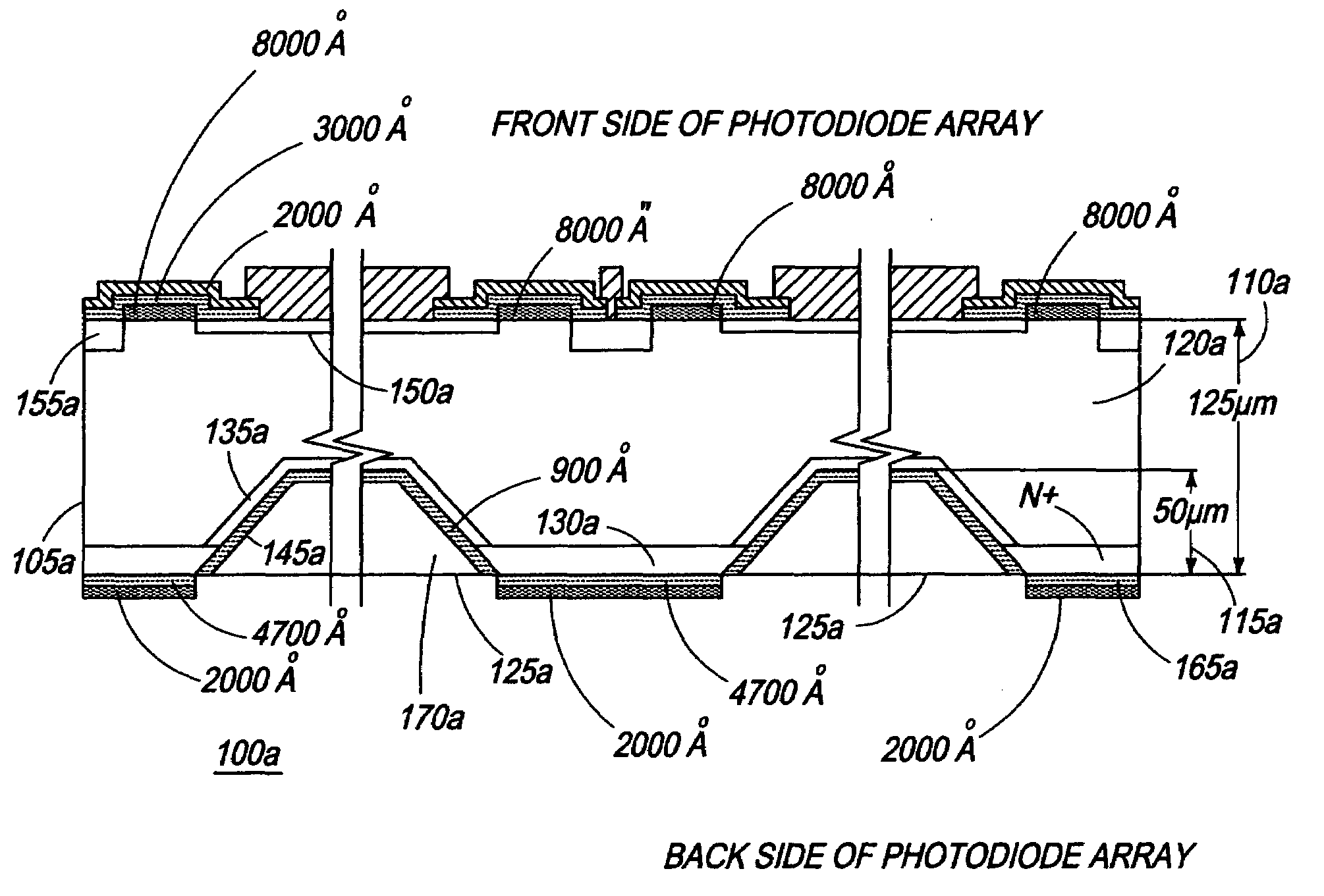
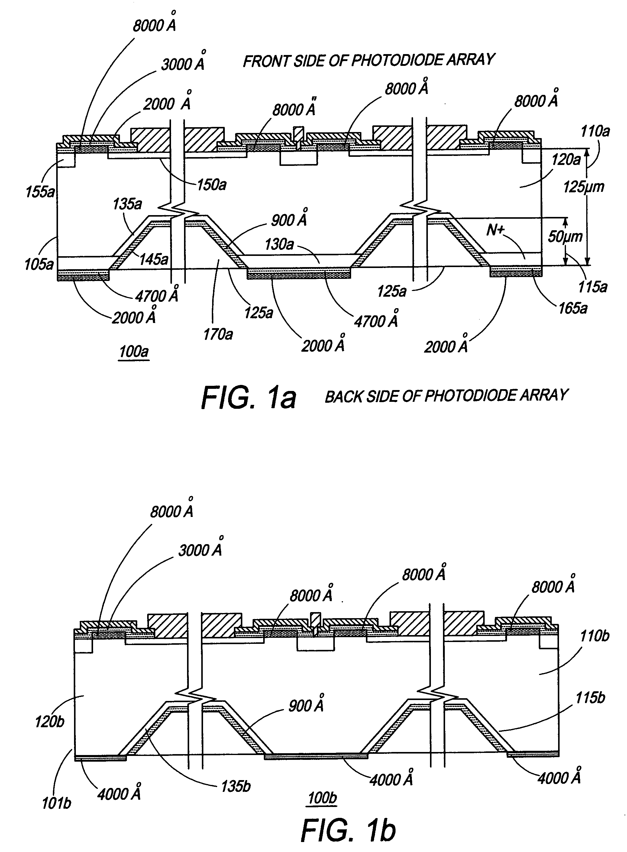
[0066]Referring now to FIG. 1b, a photodiode array 100b is depicted. Photodiode array 100b comprises first region 110b, second region 115b, and third region 120b, dimensional details of which are discussed above with reference to FIG. 1a. In addition, the doping materials used, masking layers formed, and etching techniques adopted to form the 3-D microstructures have already been explained above with reference to FIG. 1a. In the manufacture of photodiode array 100b, however, only a single first masking layer is applied to the back side of the photodiode array. For example, and by no way of limitation, the single masking layer 165b is preferably Si3N4 and of a thickness of 4000 Å. In addition, second region 115b comprises only a shallow n+ region 135b.

[0067]Referring to FIG. 3, another embodiment of the photodiode array of the present invention is illustrated. The back side illuminated, front side contact (BSL-FSC) photodiodes are implemented in an array and have superior performanc...

third embodiment

[0101]In a third embodiment, as shown in FIG. 7c, photodiode array 700c may have the following variable characteristics, assuming an x-y-z axis as drawn near photodiode 700c wherein the x-axis represents the length of the wafer, the y-axis represents the width of the wafer, and the z-axis represents the height of the wafer: p+ to n+ separation 705c in the x-direction of 0.075 mm; p+ to n+ separation 706c in a y-direction of 0.075 mm; the width between two contiguous p+ fishbone ribs 707c, also in a y-direction, of 0.109 mm; and wafer height 708c in a z-direction of approximately 0.125 mm. Also shown in FIG. 7c is periphery frame bone 709c, which surrounds the fishbone rib structure.

[0102]FIG. 8a depicts a top view of the photodiode array 800 of the present invention. Each square box represents diode elements 802 within photodiode array 800. In one embodiment, photodiode array 800 is arranged in the form of a 16 by 16 matrix with a total of 256 diode elements 802 on a silicon wafer s...


PUM

PropertyMeasurementUnit
Lengthaaaaaaaaaa
Thicknessaaaaaaaaaa
Thicknessaaaaaaaaaa

Abstract

The present invention is directed toward a detector structure, detector arrays, and a method of detecting incident radiation. The present invention comprises several embodiments that provide for reduced radiation damage susceptibility, decreased affects of crosstalk, reduced dark current (current leakage) and increased flexibility in application. In one embodiment, a photodiode array comprises a substrate having at least a front side and a back side, a plurality of diode elements integrally formed in the substrate forming the array, wherein each diode element has a p+ fishbone pattern on the front side, and wherein the p+ fishbone pattern substantially reduces capacitance and crosstalk between adjacent photodiodes, a plurality of front surface cathode and anode contacts, and wire interconnects between diode elements made through a plurality of back surface contacts.

Description

CROSS REFERENCE TO RELATED APPLICATIONS[0001]This invention relies on, for priority, U.S. patent application Ser. No. 10 / 838,897 having a filing date of May 5, 2004, entitled “THIN WAFER DETECTORS WITH IMPROVED RADIATION AND CROSSTALK CHARACTERISTICS” which further relies on Provisional Application 60 / 468,181, having a priority date of May 5, 2003, entitled “DETECTORS WITH IMPROVED RADIATION DAMAGE AND CROSSTALK CHARACTERISTICS”.FIELD OF THE INVENTION[0002]The present invention pertains generally to the field of radiation detectors, and in particular, relates to radiation detectors manufactured with a fishbone structure to reduce both capacitance and crosstalk between detecting regions.BACKGROUND OF THE INVENTION[0003]Arrays of photosensitive diodes are used in an assortment of applications including, but not limited to, radiation detection, optical position encoding, and low light-level imaging, such as night photography, nuclear medical imaging, photon medical imaging, multi-slice...

Claims


Application Information

Patent Timeline
IPC IPC(8): H01L31/0216
CPCB23K1/0016B23K2201/42H01L27/14634H01L27/14643H01L27/14692H05K3/26H01L27/1464H05K3/3442H05K3/3452H05K2201/0989H05K2201/09909H05K2201/10689H05K2201/10727H05K3/3421B23K2101/42
Inventor BUI, PETER STEVENTANEJA, NARAYAN DASS
Owner OSI OPTOELECTRONICS
Why Eureka
Try Eureka