Nitride semiconductor heterojunction field effect transistor

a semiconductor and heterojunction field technology, applied in the direction of semiconductor devices, basic electric elements, electrical appliances, etc., can solve the problems of difficult to reduce the interface state of the alsub>2/sub>osub>3/sub>/algan, and difficult to make the two-dimensional electron gas zero

Inactive Publication Date: 2008-06-12
FURUKAWA ELECTRIC CO LTD +1
View PDF3 Cites 34 Cited by
  • Summary
  • Abstract
  • Description
  • Claims
  • Application Information

AI Technical Summary

Benefits of technology

[0029]In a nitride semiconductor heterojunction field effect transistor according to a ninth aspect of the present invention, the insulator layer including the negative ions is formed of silicon nitrides.
[0030]According to the aspect, using the silicon nitrides for the insulator layer including the negative ions, the nitrogen is the element similar to that in the second nitride semiconductor layer (an AlGaN layer for instance). Hence, it becomes one of the insulator layers which have the least interface state density at the interface with the second nitride semiconductor layer. Therefore, a fluctuation of a current-voltage characteristic (decreasing of a drain current) at the time of applying a high drain bias voltage, as it is called a current collapse, is able to be suppressed.

Problems solved by technology

However, in an AlGaN / GaN HFET, due to a spontaneous polarization and a piezoelectric effect, it is difficult to make the two-dimensional electron gas be zero, when gate voltage is not applied.
Moreover, in this method, it is difficult to obtain a sufficient channel current, because a gate forward current is flowed under applying a positive bias onto the gate.
However, in the method, it is difficult to reduce an interface state of the Al2O3 / AlGaN.
Hence, electrons are trapped at the interface, and then channel charges are not able to be increased.
Hence, a controllability as a device becomes worse.
For instance, it is difficult to control a threshold voltage in accurate, so as to make the drain current be zero, even when some amount of positive voltage is applied onto the gate.

Method used


Image

  • Nitride semiconductor heterojunction field effect transistor
  • Nitride semiconductor heterojunction field effect transistor
  • Nitride semiconductor heterojunction field effect transistor

Examples


first embodiment

THE FIRST EMBODIMENT

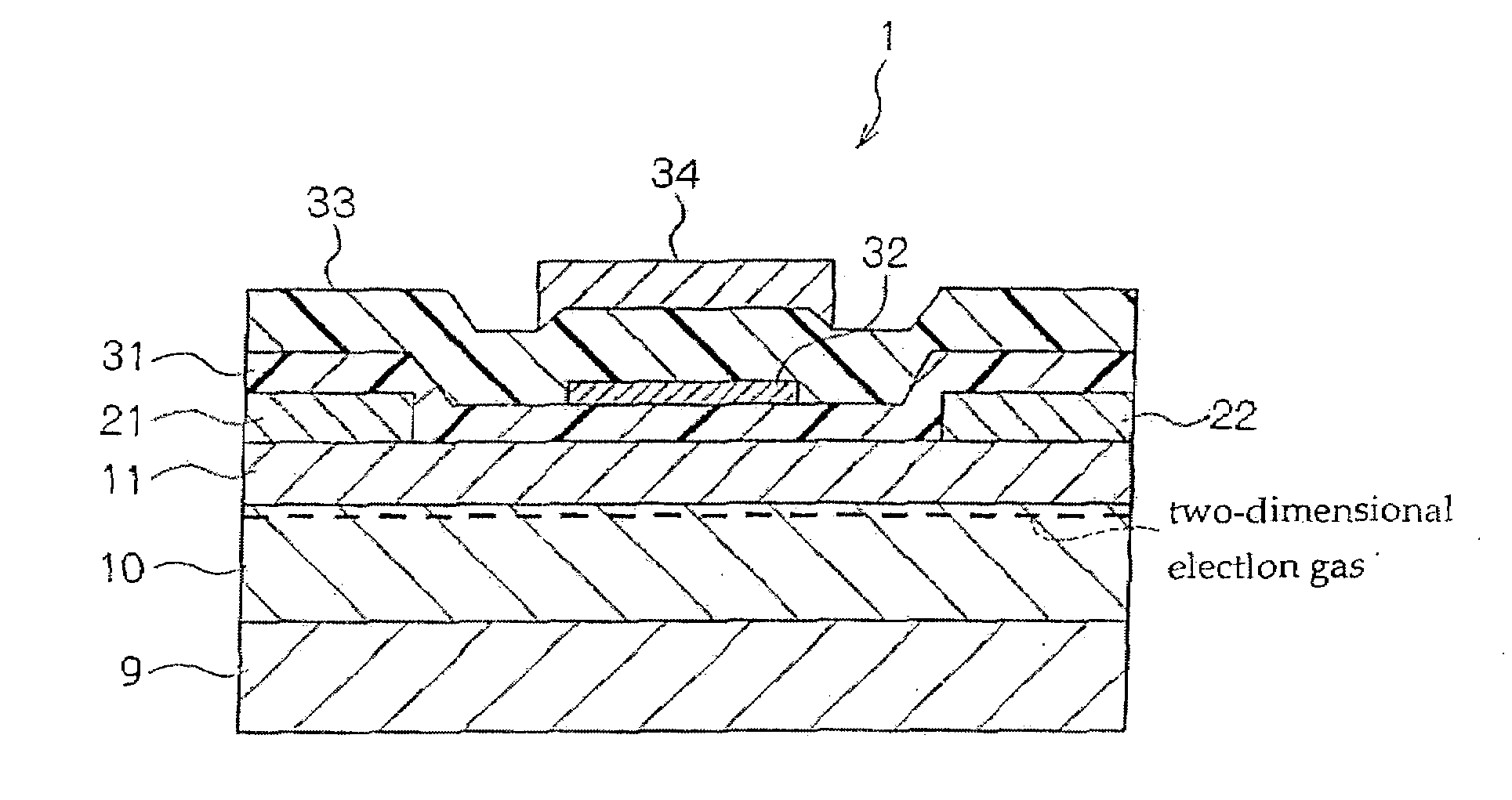
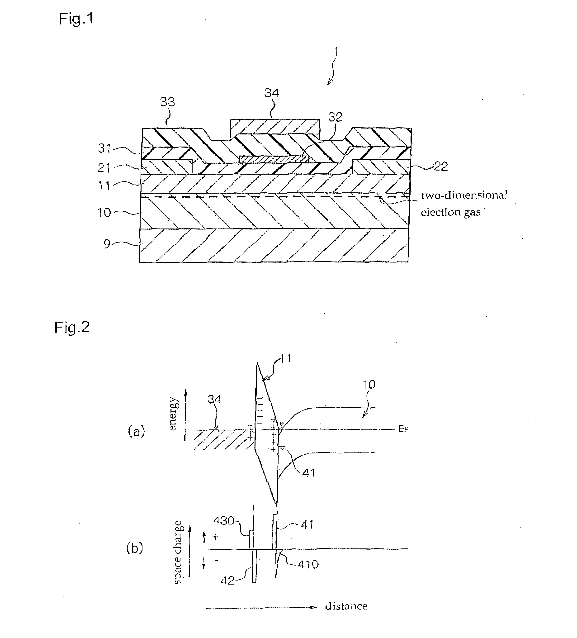
[0048]FIG. 1 shows a schematic structure of an AlGaN / GaN HFET (1) regarding the first embodiment. The AlGaN / GaN HFET (1) comprises a sapphire substrate (9), a GaN layer (10) formed on the sapphire substrate (9), an AlGaN layer (11) formed on the GaN layer (10), a source electrode (21), and a drain electrode (22). Moreover, there is provided a silicon nitride (SiNx) film (31) on an active area between the source electrode (21) and the drain electrode (22), using a catalytic chemical vapor deposition (a cat CVD) method.

[0049]In the AlGaN / GaN HFET (1), a heterojunction interface is formed by the AlGaN layer (11) having a wide band gap and the GaN layer (10) having a narrower band gap than that of the AlGaN layer (11).

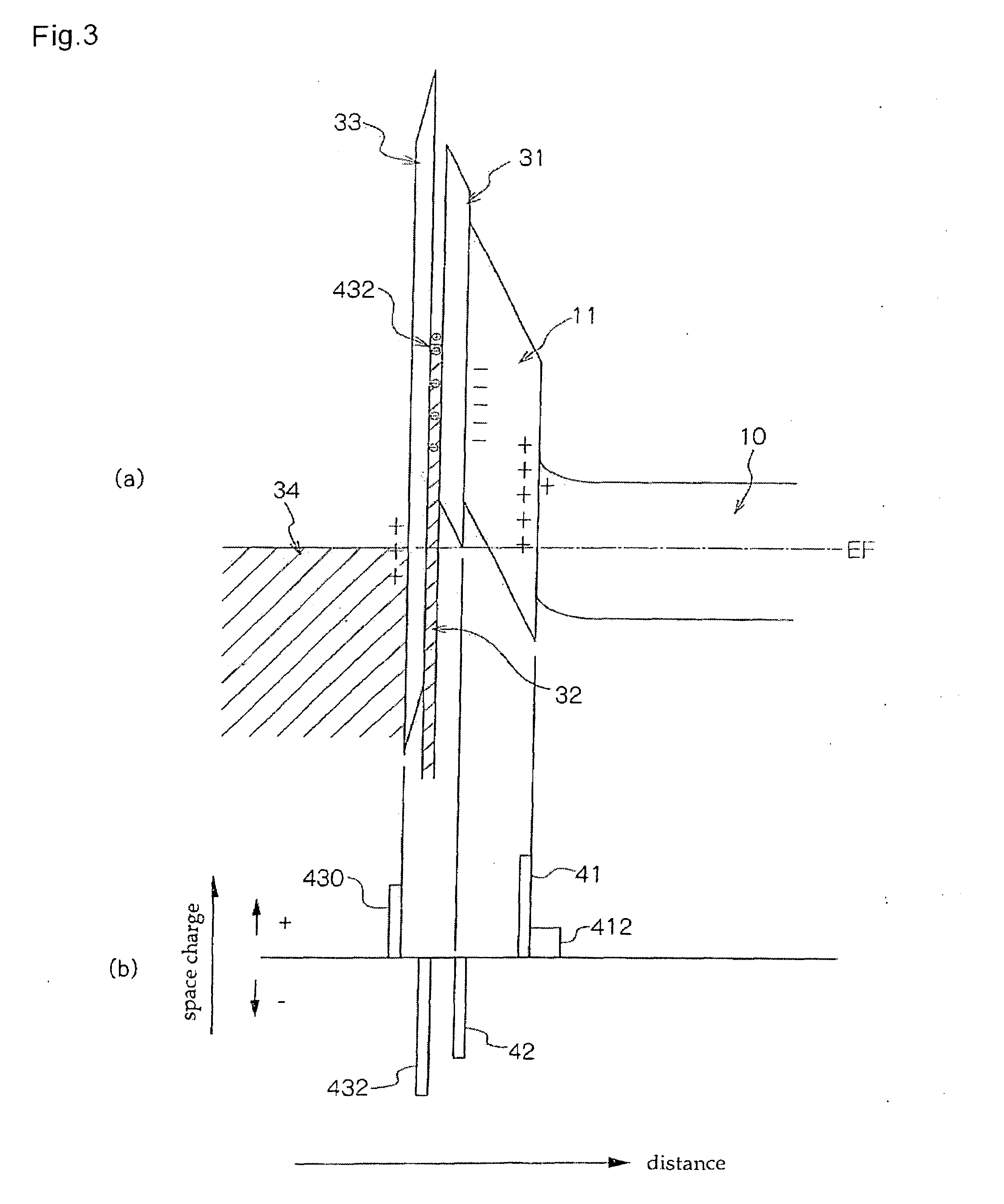
[0050]On the silicon nitride film layer (31), there is provided a floating gate layer (32) at an area inferior to a control gate electrode (34). Moreover, the floating gate layer (32) is, as an example for the embodiment, formed using a low resistance p...

second embodiment

THE SECOND EMBODIMENT

[0067]FIG. 8 shows a schematic structure of an AlGaN / GaN HFET (1A) according to the second embodiment. In the AlGaN / GaN HFET (1A), there is provided the silicon nitride (SiNx) film (31) on an active area of the ordinary AlGaN (11) / GaN (10) HFET, using a catalytic chemical vapor deposition (Cat CVD) method, as similar to the first embodiment.

[0068]In a region directly under a gate (312) of the silicon nitride film layer (31), using such as ion implantation or the like, negative ions, such as Cl− or the like, are added. Moreover, in the AlGaN / GaN HFET (1A), different from the first embodiment as shown in FIG. 1, the control gate electrode (34) is formed directly on the silicon nitride film layer (31). Furthermore, by controlling the amount of the negative ions adding into the silicon nitride film layer (31), the threshold voltage of the AlGaN / GaN HFET (1A) is able to be freely controlled. Other portions in the structure are similar to the first embodiment as shown...


PUM


Abstract

In the nitride semiconductor heterojunction field effect transistor of the present invention, the floating gate layer (32), as the third layer, is formed between the control gate electrode (34) and the AlGaN layer (11), and the potential for the electrons in the AlGaN layer (11), which is substantially neighboring the floating gate layer (32), is able to be substantially high, and then the channel is able to be depleted. Hence, no current can be flowed through the channel (no drain current) at the time of no gate voltage, as so-called stable normally-off operation can be obtained.

Description

BACKGROUND OF THE INVENTION[0001]1. Technical Field[0002]The present invention relates to a nitride semiconductor device, and more specifically to a nitride semiconductor heterojunction field effect transistor (FET), in which drain current is zero when gate voltage is not applied, as it is called a normally-off type.[0003]2. Related Arts[0004]A nitride semiconductor, such as GaN, AlGaN, InGaN, and the like, has greater band gap energy than the conventional semiconductors, such as Si, GaAs, and the like. Therefore, it is excellent as a semiconductor for high temperature or high breakdown voltage devices. In particular, using materials of these nitride semiconductors (GaN semiconductors), different from other wide band gap semiconductors, such as SiC or the like, it becomes possible to form a heterojunction such as AlGaN / GaN or the like. Therefore, a nitride semiconductor heterojunction field effect transistor (a heterojunction FET: HFET), or a high electron mobility transistor (HEMT)...

Claims


Application Information

Patent Timeline
Patent Type & Authority Applications(United States)
IPC IPC(8): H01L29/778
CPCH01L29/2003H01L29/207H01L29/408H01L29/518H01L29/7787H01L29/42324
Inventor YOSHIDA, SEIKOHHASEGAWA, FUMIO
Owner FURUKAWA ELECTRIC CO LTD
Why Eureka
Try Eureka