Self assembled controlled luminescent transparent conductive photonic crystals for light emitting devices

a technology of luminescent transparent conductive and self-assembling, which is applied in the direction of crystal growth process, polycrystalline material growth, instruments, etc., can solve the problems of low efficiency of silicon carbide (sic) leds, difficulty in fabricating low resistance ohmic contacts to p-type gan, and difficulty in diamond and zno based emitters. , to achieve the effect of minimizing light trapping, minimizing current spreading, and maximizing light extraction

Inactive Publication Date: 2008-06-19
STRUCTURED MATERIALS
View PDF25 Cites 19 Cited by
  • Summary
  • Abstract
  • Description
  • Claims
  • Application Information

AI Technical Summary

Benefits of technology

[0020]We have developed fabrication technology for GaN LED contacts, based on MOCVD of transparent conductive oxides. We are concentrating on TCO materials based on zinc oxide, due to their desirable properties. However, the general MOCVD process and tool technology results obtained will be equally applicable to more common TCO's

Problems solved by technology

Silicon carbide (SiC) LED's have low efficiency.
Diamond and ZnO based emitters are not yet well developed.
GaN based LED's are typically fabricated on single crystal sapphire (Al2O3) substrates, due to the lack of suitable GaN substrates.
Fabricating low resistance Ohmic contacts to p-type GaN is more difficult.
Part of the issue is the difficulty in p

Method used


Image

  • Self assembled controlled luminescent transparent conductive photonic crystals for light emitting devices
  • Self assembled controlled luminescent transparent conductive photonic crystals for light emitting devices
  • Self assembled controlled luminescent transparent conductive photonic crystals for light emitting devices

Examples


Embodiment Construction
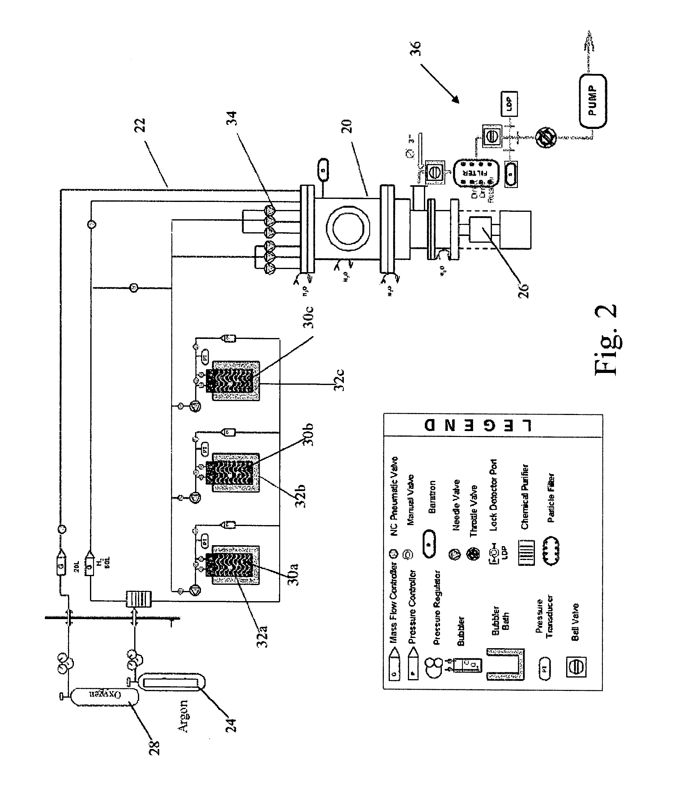
MOCVD Equipment

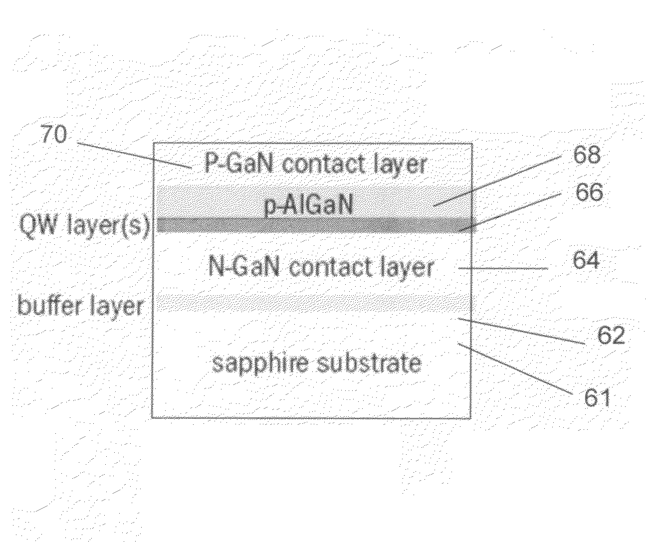
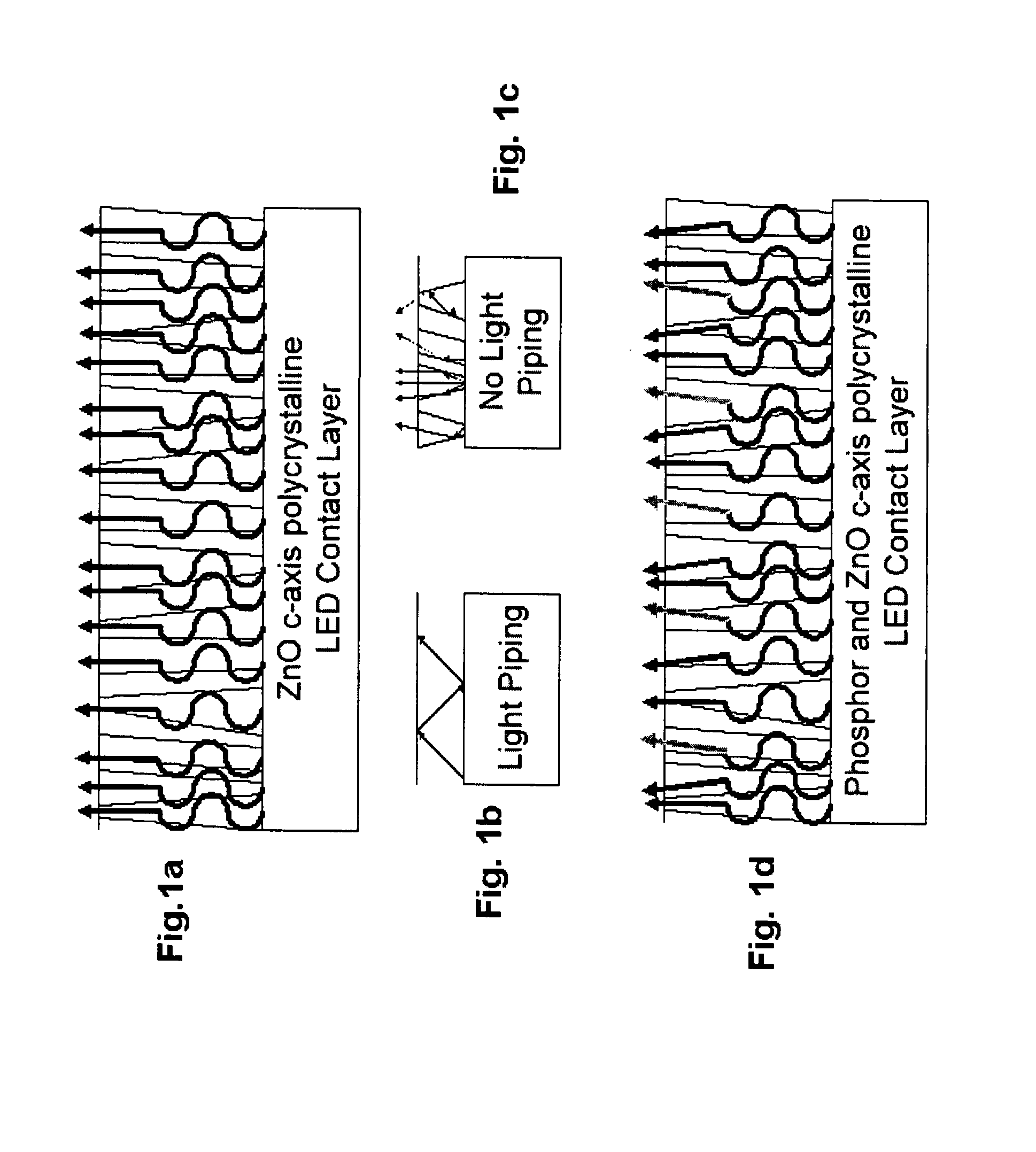
[0028]FIG. 1 of the drawings illustrates the effect of a transparent conductive film with a self assembled columnar (or semicolumnar) photonic crystal (or wire) grain structure to enhance light output from an LED. In FIG. 1A the columnar grains of MOCVD deposited ZnO channel and scatter the emitted light in a direction normal to the film surface, and minimize light loss in the direction parallel to the film surface. In FIG. 1B TCO films with equiaxed grains, or amorphous films such as ITO or ZnO films not deposited as described herein, allow lateral propagation or “light piping” of the LED emission in a direction parallel to the film surface which diminishes the usable light output from the device. FIG. 1C shows TCO films with columnar grain structures which inhibit undesirable parallel light piping. FIG. 1D shows that when combined with a thin film phosphor, the columnar grain structure of the transparent conductive oxide film results in utilization of the LED emissi...


PUM

PropertyMeasurementUnit
Temperatureaaaaaaaaaa
Angleaaaaaaaaaa
Poweraaaaaaaaaa

Abstract

A transparent conductive oxide contact layer to enhance the spectral output of a light emitting device and a methodology for its deposition. The transparent conductive oxide deposited on the light emitting device so as to have a columnar structure. The transparent conductive oxide contact layer may be preferably ZnO doped with a conductive element. Light emitting phosphors may also be deposited within the transparent conductive oxide contact layer.

Description

REFERENCE TO RELATED APPLICATIONS[0001]This application claims priority from U.S. provisional application Ser. No. 60 / 850,310 filed Oct. 10, 2006 the disclosure of which is hereby incorporated by reference.BACKGROUND OF THE INVENTION[0002]The present invention is directed to the formation of an improved transparent conductive oxide (TCO) suitable for use as a contact layer on light emitting semiconductor devices such as Light Emitting Diodes (LEDs).[0003]Light Emitting Diodes (LEDs) are an important lighting product. It is important to maximize light output efficiency and spectrum using the most economical methods. Disclosed is a technology to enhance light output efficiency, control and augment spectral output and a process to produce the disclosed technology. Further, the technology disclosed is also applicable to enhancing other light emission materials, such as organic light emitting diodes as well as being useful to enhance light absorption properties of devices.[0004]We have d...

Claims


Application Information

Patent Timeline
IPC IPC(8): H01L33/00H01L33/32H01L33/42
CPCB82Y20/00C23C16/407C23C16/4481C30B25/18H01L33/42C30B29/406G02B6/1225H01B1/16H01L33/32C30B29/16
Inventor TOMPA, GARY S.SUN, SHANGZHURICE, CATHERINE E.SBROCKEY, NICK M.PROVOST, LLOYD G.
Owner STRUCTURED MATERIALS
Why Eureka
Try Eureka