
Electron blocking layers for electronic devices

a technology of electronic devices and electron blocks, applied in the field of flash memory devices, can solve problems such as large over-erase voltages, and achieve the effect of improving performance and charge retention properties

Inactive Publication Date: 2008-06-26
SANDISK TECH LLC
View PDF99 Cites 88 Cited by
  • Summary
  • Abstract
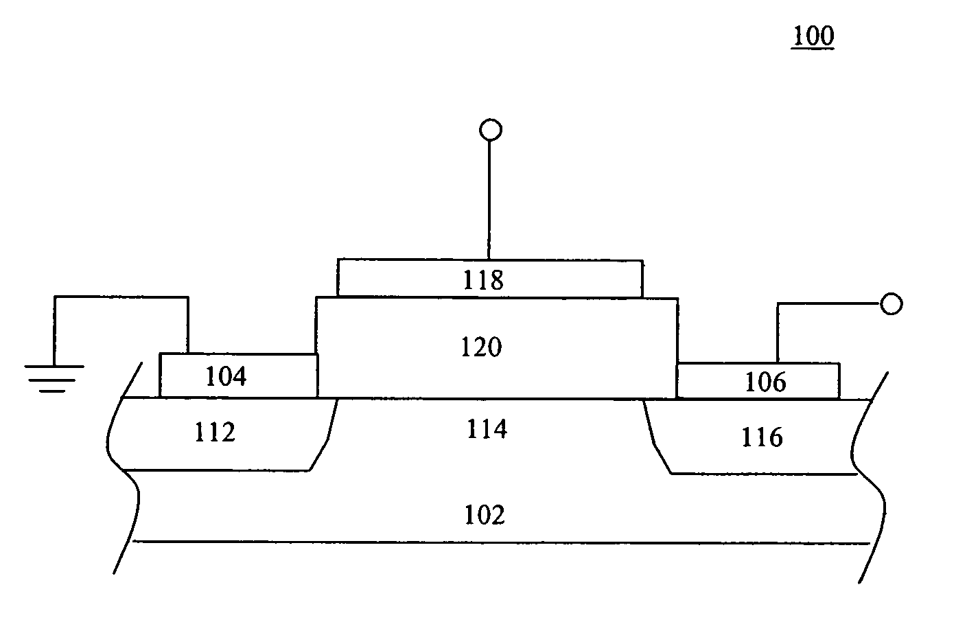
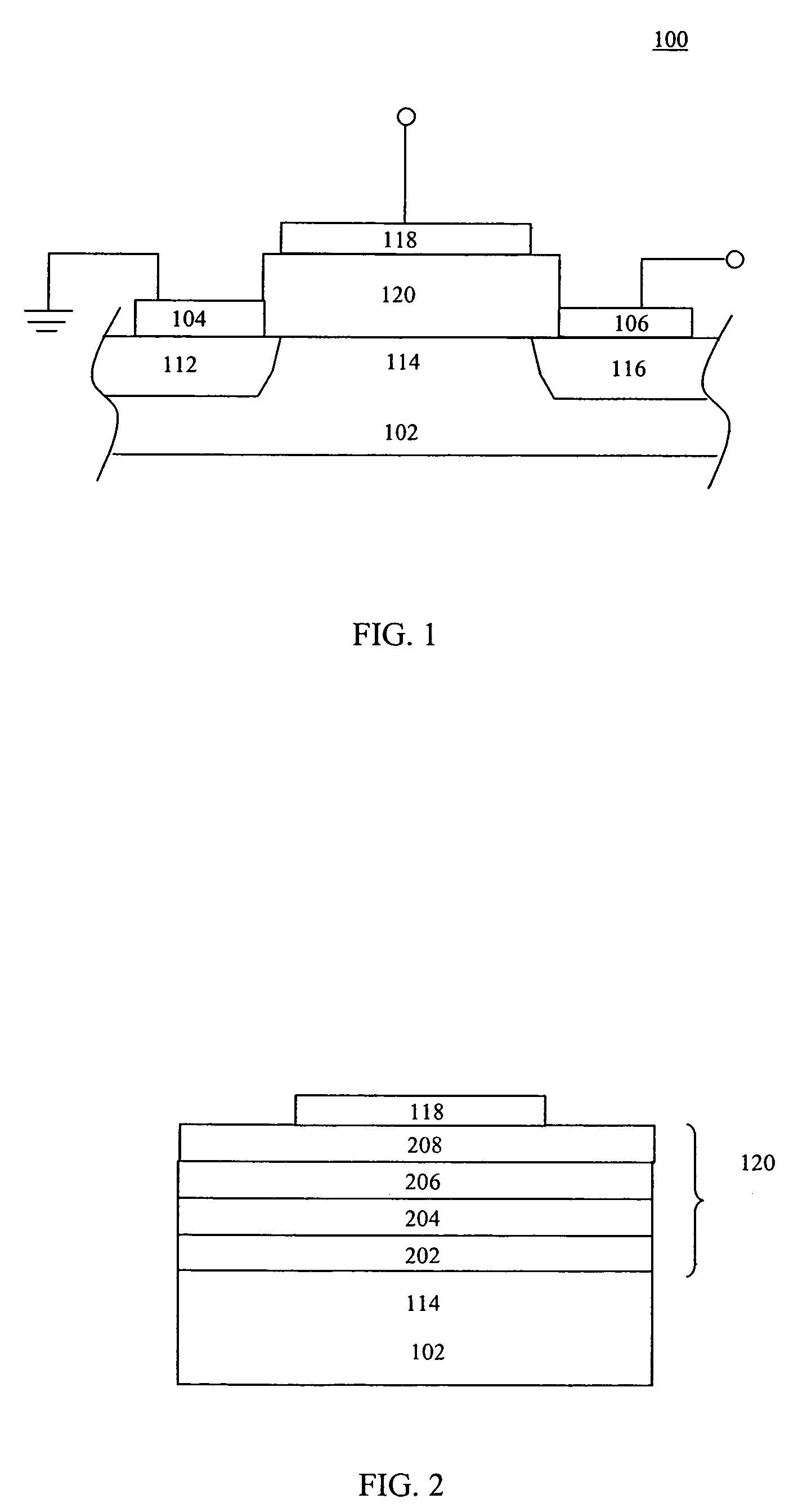
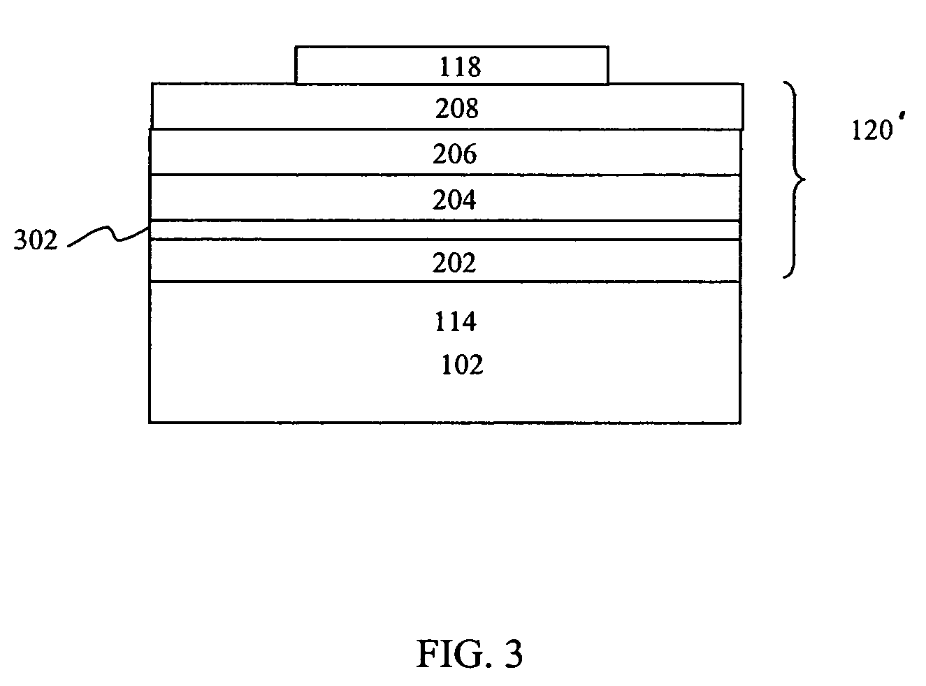
  • Description
  • Claims
  • Application Information

AI Technical Summary

Benefits of technology

[0007]The enhancement of performance and charge retention properties of nonvolatile memory devices using metal or semiconductor nanocrystals (such as colloidal quantum dots or quantum dots formed using processes such as chemical vapor deposition or physical vapor deposition) or nonconductive nitride based charge trapping layers embedded in a high-k dielectric matrix, is important to overcome the scaling limitations of conventional non-volatile memories beyond the 50 nm technology node and to fully enable reliable multi-bit operation.
[0008]The present invention relates to methods, systems and apparatuses for improved electronic devices, such as memory devices, having enhanced characteristics including increased charge retention, enhanced memory program / erase window, improved reliability and stability, with feasibility for single or multistate (e.g., two, three or four bit) operation. The use of a multi-layer control dielectric, such as a double or triple layer control dielectric, in a nonvolatile memory device is disclosed for the first time. The multi-layer control dielectric includes a combination of high-k dielectric materials such as aluminum oxide (Al2O3), hafnium oxide (HfO2), and / or hybrid films of hafnium aluminum oxide (HfAlOx, wherein x is a positive integer, e.g., 1, 2, 3, 4, etc.) therein.
[0012]The thickness of single or dual layers of HfO2 (or HfAlO3) can be kept very thin while still efficiently blocking current flow. For example, in an embodiment, the thickness is less than about 4 nm. In another example embodiment, the thickness is less than about 2 nm.
[0013]In embodiments, the use of such a double or triple layer control dielectric provides the unexpected result of achieving a very large program / erase window (e.g., on the order of about 12 volts or greater), while still providing for good charge retention and programming / erasing speed, which is important in making reliable multi-bit / cell memory devices with scaling to smaller node sizes. Furthermore, in an embodiment, the charge-blocking layer dramatically reduces the amount of current that flows through the control dielectric during the program, erase, and read operations, which enables flash memory devices that can endure a large number of program / erase cycles without significant drift in operation voltages.

Problems solved by technology

The layer of HfO2 suppresses a tunneling current from a control gate of the memory device during erase operations which can lead to large over-erase voltages.

Method used


Image

  • Electron blocking layers for electronic devices
  • Electron blocking layers for electronic devices
  • Electron blocking layers for electronic devices

Examples


example embodiments

[0055]In an example embodiment, charge storage layer 204 includes metal dots, charge blocking layer 206 is HfO2, and control dielectric layer 208 is Al2O3. FIG. 7A shows a simulation plot 700 of energy (eV) versus a thickness (nm) of a combination control dielectric of charge blocking layer 206 (HfO2) and control dielectric layer 208 (Al2O3). FIG. 7B shows a simulation plot 750 of current (A / cm2) versus electric field (V / cm). Plot 700 shows a plot line 702 for the combination control dielectric only including HfO2, and a plot line 704 for the combination control dielectric only including Al2O3. For both of plot lines 702 and 704, no barrier lowering is indicated. Plots 700 and 750 show that including a thin layer of HfO2 at the interface of metal and Al2O3 can reduce the electron tunneling current by many orders of magnitude. This is true even if the HfO2 layer is less than 1 nm thick.

[0056]FIGS. 8A-8C respectively show plots 800, 810, and 820 related to an example gate stack simila...


PUM


Abstract

Methods and apparatuses for electronic devices such as non-volatile memory devices are described. The memory devices include a multi-layer control dielectric, such as a double or triple layer. The multi-layer control dielectric includes a combination of high-k dielectric materials such as aluminum oxide (Al2O3), hafnium oxide (HfO2), and / or hybrid films of hafnium aluminum oxide. The multi-layer control dielectric provides enhanced characteristics, including increased charge retention, enhanced memory program / erase window, improved reliability and stability, with feasibility for single or multistate (e.g., two, three or four bit) operation.

Description

BACKGROUND OF THE INVENTION[0001]1. Field of the Invention[0002]The present invention relates to memory devices, and more particularly, to flash memory devices.[0003]2. Background Art[0004]Non-volatile memory devices, such as flash memory devices, are memory devices that can store information even when not powered. A flash memory device stores information in a charge storage layer that is separated from a “control gate.” A voltage is applied to the control gate to program and erase the memory device by causing electrons to be stored in, and discharged from the charge storage layer.[0005]A control dielectric is used to isolate the control gate from the charge storage layer. It is desirable for the control dielectric to block charge flow between the charge storage layer and control gate. High-k dielectric layers can serve as efficient charge-blocking layers. They have been used as the control dielectric layer for flash memory devices, such as Samsung's TANOS devices, to enable the dow...

Claims


Application Information

Patent Timeline
IPC IPC(8): H01L29/792H01L21/336
CPCH01L29/42324H01L29/7881H01L29/517H01L29/42332
Inventor CHEN, JIANDUAN, XIANGFENGCRUDEN, KARENLIU, CHAONALLABOLU, MADHURI L.RANGANATHAN, SRIKANTHLEON, FRANCISCOPARCE, J. WALLACE
Owner SANDISK TECH LLC
Learn More