Mask Patterns for Semiconductor Device Fabrication and Related Methods and Structures

a semiconductor device and mask pattern technology, applied in the field of mask pattern for semiconductor device fabrication, can solve the problems of deteriorating dry etching characteristics, difficult to satisfy resolution and dry etching characteristics simultaneously, etc., and achieve the effect of ensuring the vertical sidewall profile of the mask pattern remains relatively unchanged, sufficient resistance to dry etching, and simple and inexpensive process

Inactive Publication Date: 2008-07-24
SAMSUNG ELECTRONICS CO LTD
View PDF15 Cites 34 Cited by
  • Summary
  • Abstract
  • Description
  • Claims
  • Application Information

AI Technical Summary

Benefits of technology

[0024]According to some embodiments of the present invention, an organic-inorganic hybrid siloxane network film may be a sol-gel reaction product induced by an acid of a resist pattern. The organic-inorganic hybrid siloxane network film may be formed on the resist pattern to obtain a mask pattern with microdimensional openings above a wavelength limit established by photolithography. Therefore, a vertical sidewall profile of the mask pattern can be maintained relatively unchanged. Furthermore, a residual reactant after formation of the siloxane network film may be removed using a deionized water rinse (a relatively simple and inexpensive process). Moreover, because an underlayer may be etched using the siloxane network film as the mask pattern, a sufficient resistance to dry etching may be provided.

Problems solved by technology

However, it may be difficult to simultaneously satisfy resolution and dry etching characteristics.
A reduced resist film thickness, however, may deteriorate dry etching characteristics.

Method used


Image

  • Mask Patterns for Semiconductor Device Fabrication and Related Methods and Structures
  • Mask Patterns for Semiconductor Device Fabrication and Related Methods and Structures
  • Mask Patterns for Semiconductor Device Fabrication and Related Methods and Structures

Examples


example 1

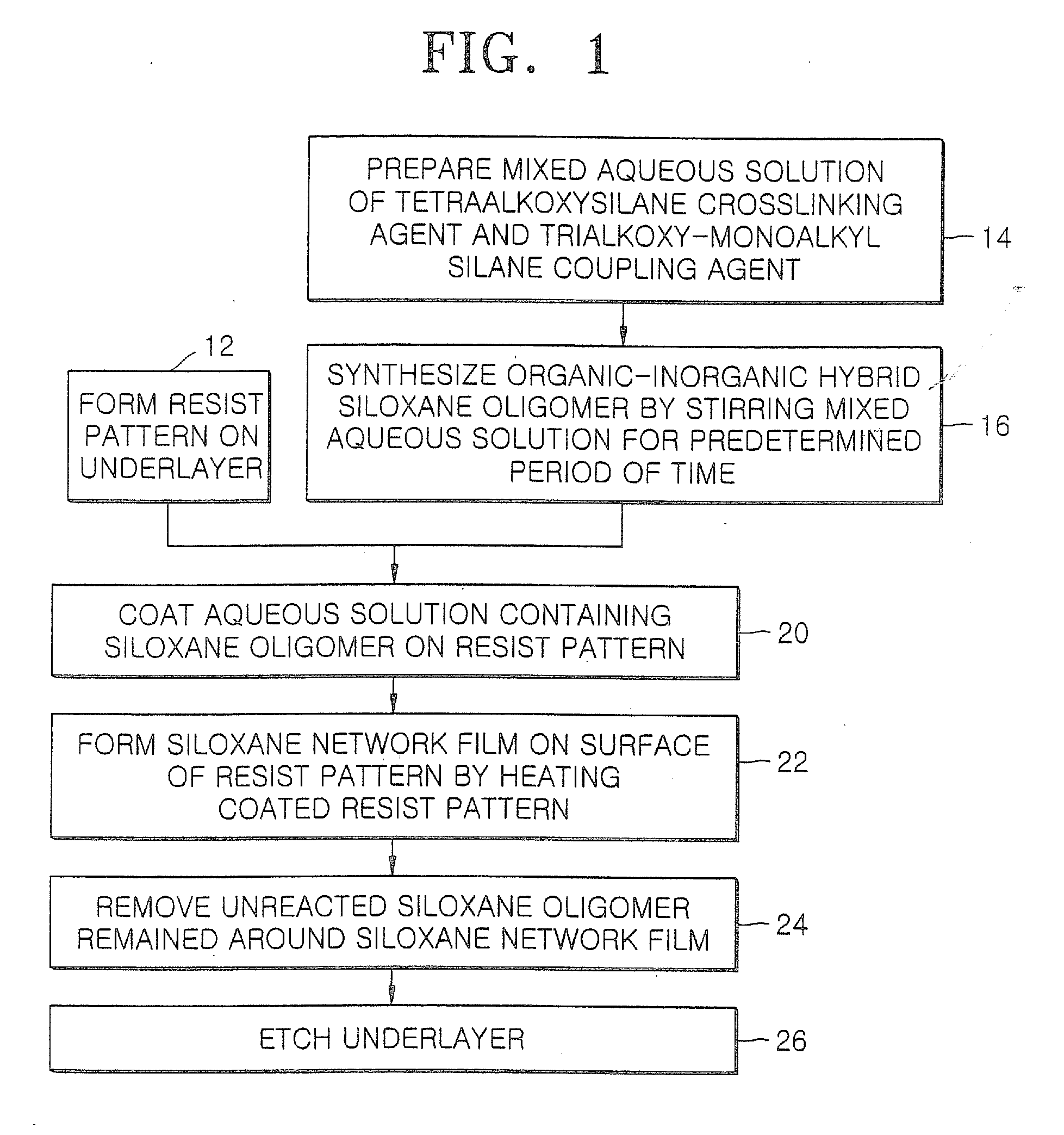
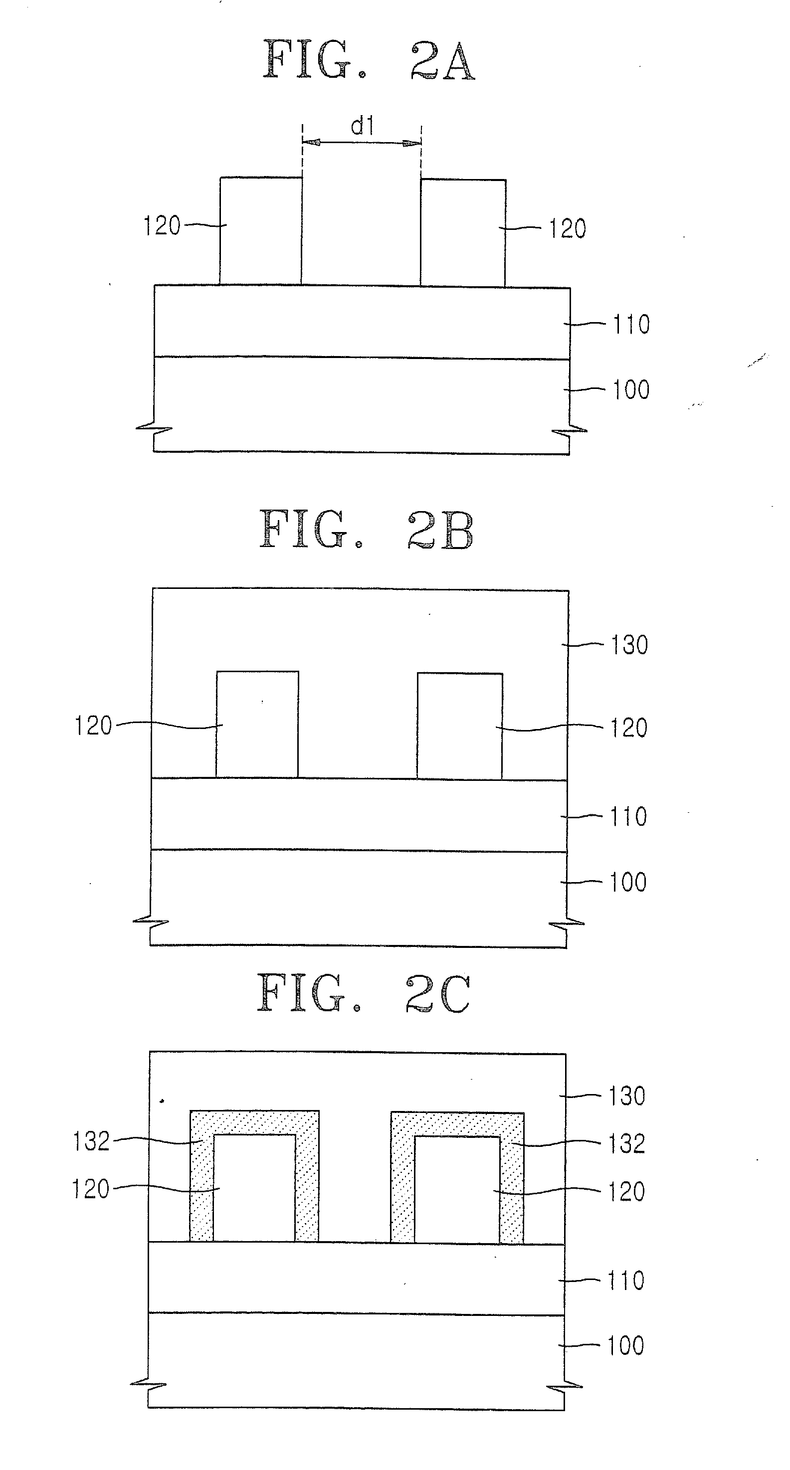
[0053]Organic antireflective films (such as DUV-30, Nissan Chemical Industries, Ltd.) were formed to thicknesses of 36 nm on bare silicon wafers and photoresists (such as SAIL-G24c, ShinEtsu Chemical Co. Ltd.) were coated thereon to form resist films with thicknesses of 240 nm. The wafers, on which the resist films were formed, were subjected to soft baking. The films thus formed were classified into five sample groups. The sample groups were subjected to exposure with ArF (193 nm) stepper (ASML 1100) specified with numeric aperture (NA) of 0.75 (annular illumination: 0.85-0.55) and exposure light energy of 22 mJ / cm2, 23 mJ / cm2, 24 mJ / cm2, 25 mJ / cm2, and 26 mJ / cm2, respectively. The sample groups were then subjected to post-exposure baking (PEB). The five sample groups were then developed with a 2.38 wt % tetramethylammonium hydroxide (TMAH) solution to form, on the wafers, resist patterns with openings defining hole patterns with CDs (critical dimensions) of 97.9 nm, 109.6 nm, 122....

example 2

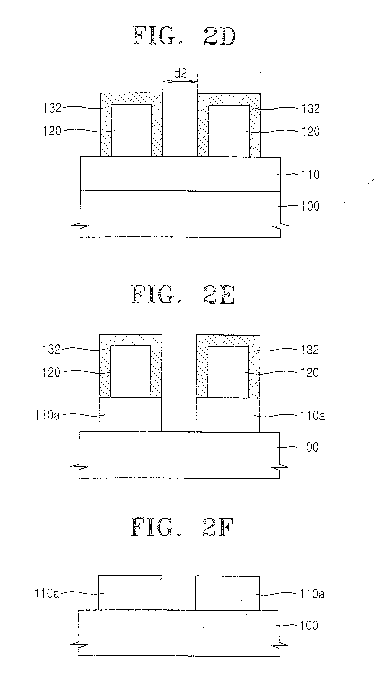
[0055]Siloxane network films for five sample groups were formed on resist patterns in the same manner as in Example 1 except that wafers coated with a siloxane oligomer-containing aqueous solution were heated at 110° C. for 60 seconds. CDs of the openings of the resist patterns exposed by the siloxane network films were 83.0 nm, 91.5 nm, 96.8 nm, 103.6 nm, and 111.7 nm for the five sample groups, respectively. In comparison with the results of Example 1, an increase of a heating temperature in this Example increased the thickness of the siloxane network films formed on surfaces of the resist patterns, so that the CDs of the openings were further reduced with increased temperatures.

[0056]According to embodiments to the present invention, an organic-inorganic hybrid siloxane network film (which is a sol-gel reaction product induced by an acid of a resist pattern) may be formed on the resist pattern to provide a mask pattern with microdimensional openings above a wavelength limit for p...


PUM

PropertyMeasurementUnit
temperatureaaaaaaaaaa
thicknessesaaaaaaaaaa

Abstract

Methods of forming an integrated circuit device may include forming a resist pattern on a layer of an integrated circuit device with portions of the layer being exposed through openings of the resist pattern. An organic-inorganic hybrid siloxane network film may be formed on the resist pattern. Portions of the layer exposed through the resist pattern and the organic-inorganic hybrid siloxane network film may then be removed. Related structures are also discussed.

Description

RELATED APPLICATION[0001]The present application claims the benefit of priority as a divisional of U.S. application Ser. No. 11 / 232,703 filed Sep. 22, 2005, which claims the benefit of priority from Korean Patent Application No. 10-2004-0076349, filed on Sep. 23, 2004, in the Korean Intellectual Property Office. The disclosures of both of the above-referenced applications are incorporated herein in their entirety by reference.FIELD OF THE INVENTION[0002]The present invention relates to semiconductor device fabrication, and more particularly to mask patterns for semiconductor device fabrication and related methods and structures.BACKGROUND[0003]In a conventional patterning process for semiconductor device fabrication, a photoresist pattern may be formed on a film (for example, a silicon film, a dielectric film, or a conductive film) to be etched for pattern formation. The film may be etched using the photoresist pattern as an etching mask to form a desired pattern.[0004]With increase...

Claims


Application Information

Patent Timeline
Patent Type & Authority Applications(United States)
IPC IPC(8): G03C3/00G03F1/70G03F1/80G03F7/40H01L21/027
CPCG03F7/405H01L21/31144H01L21/0274H01L21/0273
Inventor HAH, JUNG-HWANKIM, HYUN-WOOHATA, MITSUHIROWOO, SANG-GYUN
Owner SAMSUNG ELECTRONICS CO LTD
Why Eureka
Try Eureka