Nano-imprinting mold, method of manufacture of nano-imprinting mold, and recording medium manufactured with nano-imprinting mold

a nano-imprinting mold and manufacturing method technology, applied in the field of nano-imprinting molds, can solve the problems of low throughput, limit to pattern fineness, and high cost of equipment, and achieve the effect of increasing the ratio of depression line width, increasing the signal intensity, and increasing the resistan

Inactive Publication Date: 2008-08-07
FUJI ELECTRIC DEVICE TECH CO
View PDF4 Cites 20 Cited by
  • Summary
  • Abstract
  • Description
  • Claims
  • Application Information

AI Technical Summary

Benefits of technology

[0017]The mold can be used to manufacture a variety of products including recording medium, and specifically magnetic recording medium. By means of this invention, when the protrusion lines of a child mold are made finer without changing the pitch, the ratio of the depression line width can be increased. This means that the ratio of protrusion line widths in the resist can be increased, and that the ratio of protrusion line widths in the magnetic recording medium can be raised, so that signals with a higher signal intensity can be obtained, and a higher S / N can be obtained.

Problems solved by technology

However, EB lithography methods require expensive equipment, and because time is required to draw patterns, throughput is low, and therefore problems occur when trying to apply this process to mass production applications.
There are two major problems when applying the above-described nano-imprinting methods to machining of discrete track media, patterned media, and semiconductor devices.
One problem is that of the limit to pattern fineness.
A second problem is the fact that molds fabricated by the EB lithography method are extremely expensive.
This is because of the limit to focusing of an electron beam, because in fine patterning the power density is low and more time is required for patterning, and because as the patterning time is lengthened, shifts caused by external disturbances tend to occur.
Also, because signals are only obtained from protruding portions of the magnetic recording layer, protruding portions cannot be made smaller than necessary.
As explained above, in machining to form fine lines, the power density is low and machining times are lengthened, so that expensive EB equipment must be used for a long period of time.
This is because, in the course of repeated pattern transfers, molds are deformed and precision is degraded.
Amortization costs for expensive molds are then added to the unit cost of the manufactured products.

Method used


Image

  • Nano-imprinting mold, method of manufacture of nano-imprinting mold, and recording medium manufactured with nano-imprinting mold
  • Nano-imprinting mold, method of manufacture of nano-imprinting mold, and recording medium manufactured with nano-imprinting mold
  • Nano-imprinting mold, method of manufacture of nano-imprinting mold, and recording medium manufactured with nano-imprinting mold

Examples


example 1

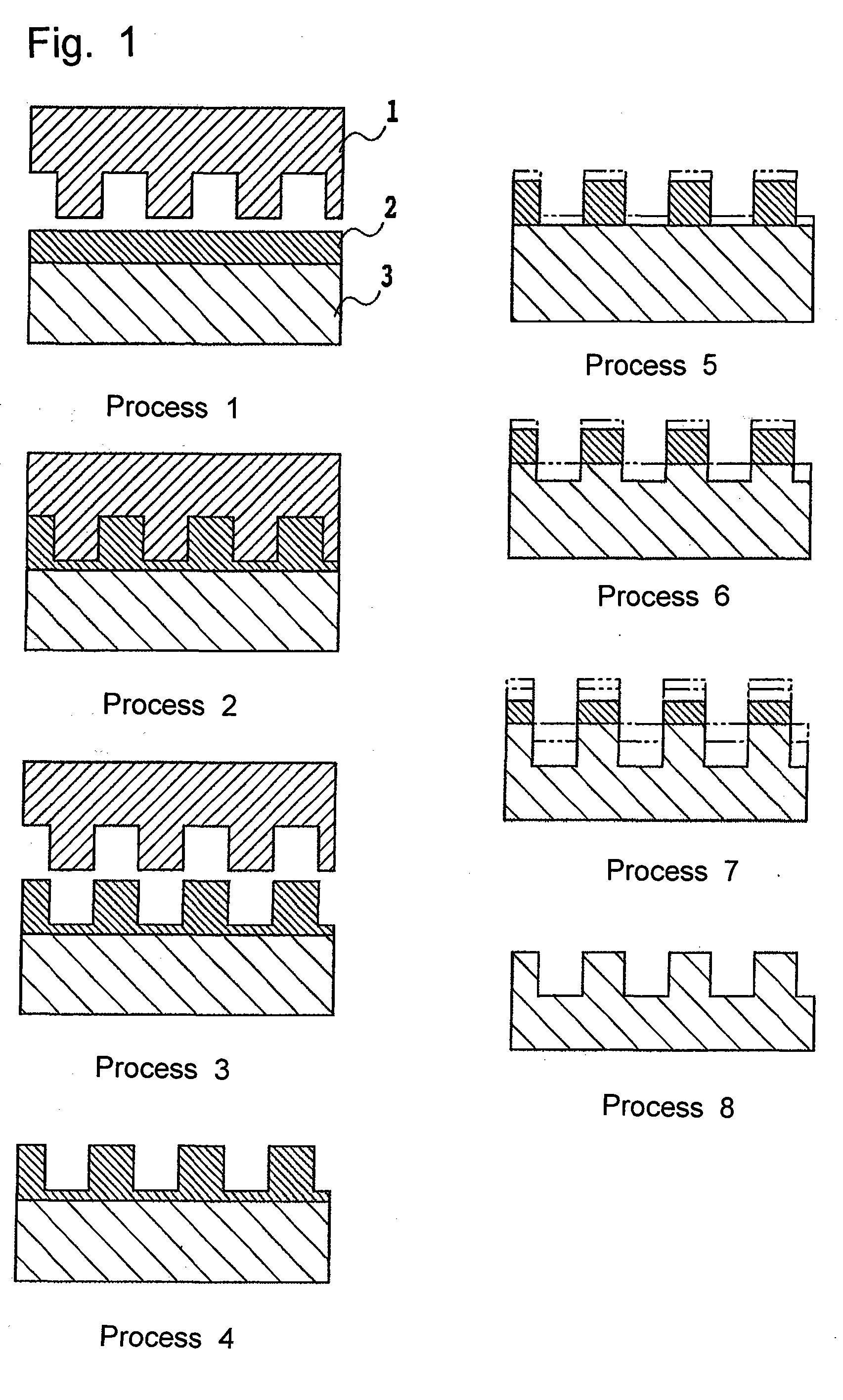
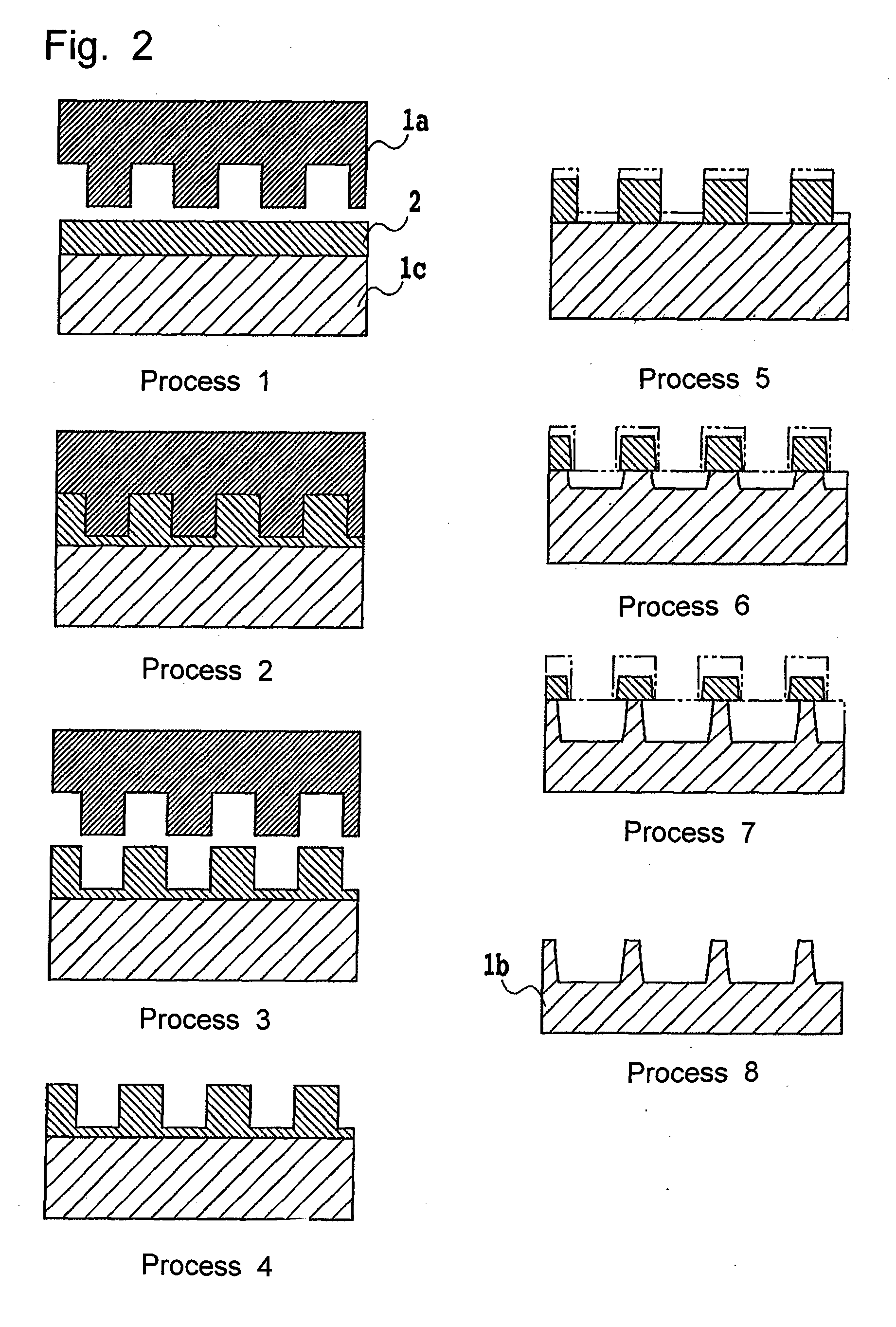
[0037]First, a quartz glass parent mold 1a was prepared as shown in process 1 of FIG. 2. As this parent mold 1a, an EB photolithography method was employed, in which resist was applied to the surface of quartz glass and EB exposure was used to form a pattern, after which dry etching was performed to form a relief pattern in the quartz glass; by this means a quartz glass mold for discrete track media was fabricated having concentric lines and spaces with line widths of 80 nm, space widths of 80 nm, and depths of 100 nm, as well as servo information pattern in some portions, over the entire surface of a donut-shaped disc of outer diameter 65 mm and inner diameter 20 mm. This parent mold was subjected to release film formation treatment to form a monolayer release film on the parent mold surface, by heating, evaporating, and causing a polymer-structure thin film material having a water-repellent base to be evaporation-deposited onto and react with the substrate surface in vacuum.

[0038]...

example 2

[0043]Using the method of Example 1, and employing a child mold with the line width to space width ratio varied, at a pitch of 160 nm and both under conditions with no side etching and under three sets of conditions to cause side etching, four types of discrete track media were fabricated with the line width / space width set to 80 nm / 80 nm, 100 nm / 60 nm, 120 nm / 40 nm, and 140 nm / 20 nm. The discrete track media thus fabricated were evaluated by measuring on-track magnetic recording signals. As a result, signals could be obtained from all four types of media. The larger the line width, the stronger were the signals, and satisfactory S / N ratios could be obtained.

example 3

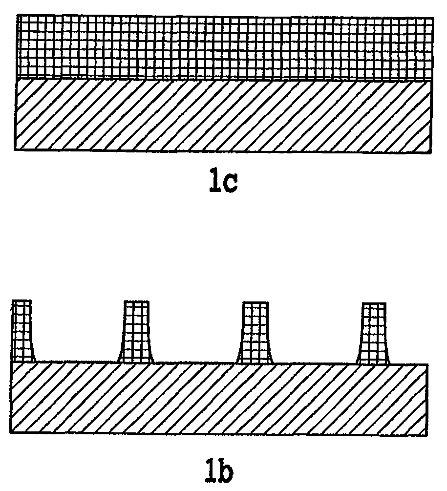
[0044]As shown in FIG. 4, a child mold was fabricated similarly to Embodiment 1, using a child mold substrate 1c prepared by sputter deposition of Ti film onto the surface of quartz glass to a thickness of 100 nm. SF6 was used as the etching gas. Etching of only the Ti film was performed, stopping at the quartz glass surface; satisfactory flat planes were obtained at the bottom portions of the depressions. Upon using this mold, similarly to Example 1, to perform nano-imprinting of a resist film (resin film) 2, a pattern with high dimensional precision could be obtained, with no sagging at the protruding portions of the resist film.


PUM

PropertyMeasurementUnit
widthaaaaaaaaaa
space widthsaaaaaaaaaa
Tgaaaaaaaaaa

Abstract

A mold is provide which, by using nano-imprinting, enables inexpensive provision of a magnetic recording medium capable of providing signals with a high signal intensity and enabling a high S/N. The method of the mold used in nano-imprinting includes: a transfer process of pressing a parent mold, having a relief pattern, against a resist layer formed on the surface of a substrate, and then releasing the parent mold to transfer the relief pattern to the resist layer; and a relief pattern formation process of exposing a lower substrate in depression portions of the resist in which the relief pattern has been formed by the transfer process, and etching the exposed substrate to form a relief pattern in the substrate, wherein in the relief pattern formation process, side etching of the substrate is performed during substrate etching.

Description

BACKGROUND[0001]The invention relates to a nano-imprinting mold, to a method of manufacture of a nano-imprinting mold, and to a magnetic recording medium manufactured with a nano-imprinting mold.[0002]Ever-finer resist patterns formed in the surfaces of substrates have been demanded with rising integration levels in the manufacture of information recording media and semiconductor devices. In the prior art, photolithography techniques have been used as methods for forming fine patterns in resist layers. In photolithography methods, a resist layer is exposed to light in order to form an exposure pattern. The resist layer is then subjected to development in order to form a pattern in the resist layer on the substrate.[0003]In order to form finer patterns in resist layers, exposure light of increasingly shorter wavelengths has been used. In order to form fine resist patterns of 100 nm or below, electron beam (EB) lithography methods, which use electron beams as the exposure radiation, h...

Claims


Application Information

Patent Timeline
Patent Type & Authority Applications(United States)
IPC IPC(8): B44C1/00B32B3/00B81C99/00
CPCB82Y10/00B82Y40/00Y10T428/24479G03F7/0017G03F7/0002
Inventor UCHIDA, SHINJI
Owner FUJI ELECTRIC DEVICE TECH CO
Why Eureka
Try Eureka